LT1336IS#TR Linear Technology, LT1336IS#TR Datasheet - Page 7
LT1336IS#TR
Manufacturer Part Number
LT1336IS#TR
Description
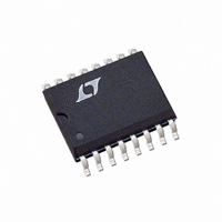
IC DRVR MOSF 1/2BRDG N-CH 16SOIC
Manufacturer
Linear Technology
Datasheet
1.LT1336CSPBF.pdf
(20 pages)
Specifications of LT1336IS#TR
Configuration
Half Bridge
Input Type
Differential
Delay Time
250ns
Current - Peak
1.5A
Number Of Configurations
1
Number Of Outputs
2
High Side Voltage - Max (bootstrap)
60V
Voltage - Supply
10 V ~ 15 V
Operating Temperature
-40°C ~ 85°C
Mounting Type
Surface Mount
Package / Case
16-SOIC (3.9mm Width)
Lead Free Status / RoHS Status
Contains lead / RoHS non-compliant
Available stocks
Company
Part Number
Manufacturer
Quantity
Price


pin FuncTions
I
An R
peak current. Pin 1 can be left open if the boost regulator
is not used.
SV
to the signal ground Pin 6.
INTOP (Pin 3): Top Driver Input. Pin 3 is disabled when
Pin 4 is high. A 3k input resistor followed by a 5V internal
clamp prevents saturation of the input transistors.
INBOTTOM (Pin 4): Bottom Driver Input. Pin 4 is disabled
when Pin 3 is high. A 3k input resistor followed by a 5V
internal clamp prevents saturation of the input transistors.
UVOUT (Pin 5): Undervoltage Output. Open collector
NPN output which turns on when V
undervoltage threshold.
SGND (Pin 6): Small-Signal Ground. Must be routed
separately from other grounds to the system ground.
PGND (Pin 7): Bottom Driver Power Ground. Connects to
source of bottom N-channel MOSFET.
BGATEFB (Pin 8): Bottom Gate Feedback. Must connect
directly to the bottom power MOSFET gate. The top
MOSFET turn-on is inhibited until Pin 8 has discharged
to below 2.5V.
SENSE
+
(Pin 2): Main Signal Supply. Must be closely decoupled
SENSE
(Pin 1): Boost Regulator I
placed between Pin 1 and V
SENSE
+
+
Comparator Input.
sets the maximum
drops below the
BGATEDR (Pin 9): Bottom Gate Drive. The high current
drive point for the bottom MOSFET. When a gate resistor
is used it is inserted between Pin 9 and the gate of the
MOSFET.
PV
to the same supply as Pin 2.
TSOURCE (Pin 11): Top Driver Return. Connects to the top
MOSFET source and the low side of the bootstrap capacitor.
TGATEFB (Pin 12): Top Gate Feedback. Must connect
directly to the top power MOSFET gate. The bottom
MOSFET turn-on is inhibited until V
has discharged to below 2.9V.
TGATEDR (Pin 13): Top Gate Drive. The high current drive
point for the top MOSFET. When a gate resistor is used it
is inserted between Pin 13 and the gate of the MOSFET.
BOOST (Pin 14): Top Driver Supply. Connects to the high
side of the bootstrap capacitor.
SWGND (Pin 15): Boost Regulator Ground. Must be routed
separately from the other grounds to the system ground.
Pin 15 can be left open if the boost regulator is not used.
SWITCH (Pin 16): Boost Regulator Switch. Connect this
pin to the inductor/diode of the boost regulator network.
Pin 16 can be left open if the boost regulator is not used.
+
(Pin 10): Bottom Driver Supply. Must be connected
TGATE FB
LT1336
– V
TSOURCE
1336fa
7
Related parts for LT1336IS#TR
Image
Part Number
Description
Manufacturer
Datasheet
Request
R

Part Number:
Description:
Half-Bridge N-Channel Power MOSFET Driver with Boost Regulator
Manufacturer:
Linear Technology
Datasheet:
Part Number:
Description:
CD ROM LINEARVIEW DATASHEETS
Manufacturer:
Linear Technology

Part Number:
Description:
Standalone Linear Li-Ion Battery Charger with Thermal Regulation in ThinSOT
Manufacturer:
Linear Technology Corporation
Datasheet:
Part Number:
Description:
Low noise, high frequency, 8th order linear phase lowpass filter
Manufacturer:
Linear Technology Corporation
Datasheet:
Part Number:
Description:
Manufacturer:
Linear Technology Corporation
Datasheet:
Part Number:
Description:
Manufacturer:
Linear Technology Corporation
Datasheet:
Part Number:
Description:
Manufacturer:
Linear Technology Corporation
Datasheet:
Part Number:
Description:
Manufacturer:
Linear Technology Corporation
Datasheet:
Part Number:
Description:
Manufacturer:
Linear Technology Corporation
Datasheet:
Part Number:
Description:
Manufacturer:
Linear Technology Corporation
Datasheet:
Part Number:
Description:
Manufacturer:
Linear Technology Corporation
Datasheet:
Part Number:
Description:
Dual and Quad, JFET Input Precision High Speed Op Amps
Manufacturer:
Linear Technology Corporation
Datasheet:
Part Number:
Description:
Manufacturer:
Linear Technology Corporation
Datasheet:
Part Number:
Description:
1, 2, 6 and 8 Channel, 10-Bit Serial I/O Data Acquisition Systems
Manufacturer:
Linear Technology Corporation
Datasheet:
Part Number:
Description:
Manufacturer:
Linear Technology Corporation
Datasheet: