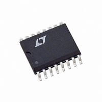
LT1336IS#TR Linear Technology, LT1336IS#TR Datasheet

LT1336IS#TR
Specifications of LT1336IS#TR
Available stocks
Related parts for LT1336IS#TR
LT1336IS#TR Summary of contents
Page 1
... MOSFETs from being partially turned on. The 0.5V hysteresis allows reliable operation even with slowly varying supplies. L, LT, LTC, LTM, Linear Technology and the Linear logo are registered trademarks of Linear Technology Corporation. All other trademarks are the property of their respective owners. 16 ...
Page 2
... LT1336IN#TRPBF LT1336CS#PBF LT1336CS#TRPBF LT1336IS#PBF LT1336IS#TRPBF Consult LTC Marketing for parts specified with wider operating temperature ranges. Consult LTC Marketing for information on non-standard lead based finish parts. For more information on lead free part marking, go to: For more information on tape and reel specifications, go to: 2 Switch Voltage (Pin 16) .............................. – ...
Page 3
T Feedback pins connected to Gate Drive pins unless otherwise specified. SYMBOL PARAMETER I DC Supply Current (Note Boost Current (Note 3) BOOST V Input Logic Low IL V ...
Page 4
LT1336 elecTrical characTerisTics temperature range, otherwise specifications are at T Feedback pins connected to Gate Drive pins unless otherwise specified. SYMBOL PARAMETER t Top Gate Lockout Delay D3 Bottom Gate Lockout Delay t Top Gate Release Delay D4 Bottom Gate ...
Page 5
Typical perForMance characTerisTics DC + Dynamic Supply Current vs Input Frequency 60 50% DUTY CYCLE C = 3000pF GATE 20V 15V + V = 10V 100 ...
Page 6
LT1336 Typical perForMance characTerisTics Top Gate Rise Time vs Temperature 300 + V = 12V 280 C = 10000pF LOAD 260 240 220 200 180 160 C = 3000pF LOAD 140 120 C = 1000pF LOAD 100 80 –50 –25 ...
Page 7
FuncTions I (Pin 1): Boost Regulator I SENSE SENSE An R placed between Pin 1 and V SENSE peak current. Pin 1 can be left open if the boost regulator is not used (Pin 2): Main Signal ...
Page 8
LT1336 FuncTional DiagraM + SENSE – 6V 480mV + 2 BIAS INTOP 5V 3k INBOTTOM 4 5V UVOUT 5 SGND 6 7 PGND BGATEFB 8 8 TRIP = 10.6V TOP UV TRIP = ...
Page 9
TesT circuiT V/I 1µ SUMIDA RCR-664D-221KC TiMing DiagraM 2V INTOP 0.8V 2V INBOTTOM 0.8V 12V TOP GATE DRIVER 12V 10V BOTTOM GATE 2V DRIVER 1N4148 200µH* ...
Page 10
LT1336 operaTion (Refer to Functional Diagram) The LT1336 incorporates two independent driver chan- nels with separate inputs and outputs. The inputs are TTL/CMOS compatible; they can withstand input voltages + as high The 1.4V input threshold is ...
Page 11
In applications where switching is always above 10kHz and the duty cycle never exceeds 90%, Pins 1, 15 and 16 can be left open. The bootstrap capacitor is then charged by conventional bootstrapping. Only a diode needs to ...
Page 12
LT1336 applicaTions inForMaTion Using the components as shown in Figure 2 the flyback regulator will run at around 800kHz. To lower the frequency C can be increased and to increase the frequency FILTER C can be decreased. FILTER D1 1N4148 ...
Page 13
Paralleling MOSFETs When the above calculations result in a lower R than is economically feasible with a single MOSFET, two or more MOSFETs can be paralleled. The MOSFETs will inherently share the currents according to their R ratio ...
Page 14
LT1336 applicaTions inForMaTion V ( OUT Switch On= Total Period HV HV–V ( OUT Switch Off= Total Period HV Note that for HV > the switch ...
Page 15
This can be avoided by placing a discharge resistor between HV supply and ground to divert the return current to ground as shown in Figure 5. For a ...
Page 16
LT1336 Typical applicaTions 100µF 10k + IN 0.0033µ 0.1µ LT1015 100k 1µF 3 0.1µ 0.0033µ 47µ 47µF 4 95k LT1058 10k ...
Page 17
DescripTion .300 – .325 (7.620 – 8.255) .008 – .015 (0.203 – 0.381) +.035 .325 –.015 ( ) +0.889 8.255 –0.381 NOTE: INCHES 1. DIMENSIONS ARE MILLIMETERS *THESE DIMENSIONS DO NOT INCLUDE MOLD FLASH OR PROTRUSIONS. MOLD FLASH OR ...
Page 18
LT1336 package DescripTion .050 BSC N .245 MIN .030 ±.005 TYP RECOMMENDED SOLDER PAD LAYOUT .010 – .020 × 45° (0.254 – 0.508) .008 – .010 (0.203 – 0.254) .016 – .050 (0.406 – 1.270) NOTE: INCHES ...
Page 19
... Updated Notes in Electrical Characteristics section. Updated Related Parts. Information furnished by Linear Technology Corporation is believed to be accurate and reliable. However, no responsibility is assumed for its use. Linear Technology Corporation makes no representa- tion that the interconnection of its circuits as described herein will not infringe on existing patent rights. LT1336 ...
Page 20
... Separate Input Channels, 100V Maximum Input Voltage, MSOP-8 www.linear.com ● 12V 2200µF EA LOW ESR 40V IRFZ34 0.1µF 12 330k 47µH 0.007 IRFZ44 IRFZ44 9 MBR340 LT 1010 REV A • PRINTED IN USA LINEAR TECHNOLOGY CORPORA TION 1996 5V 5400µF LOW ESR 1136 F08 1336fa ...


