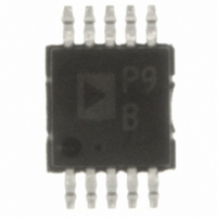
ADP3419JRMZ-REEL ON Semiconductor, ADP3419JRMZ-REEL Datasheet - Page 2

ADP3419JRMZ-REEL
Manufacturer Part Number
ADP3419JRMZ-REEL
Description
IC MOSFET DVR DUAL BOOTST 10MSOP
Manufacturer
ON Semiconductor
Type
High Side/Low Sider
Datasheet
1.ADP3419JRMZ-REEL.pdf
(10 pages)
Specifications of ADP3419JRMZ-REEL
Configuration
High and Low Side, Synchronous
Input Type
PWM
Delay Time
32ns
Current - Peak
1A
Number Of Configurations
1
Number Of Outputs
2
High Side Voltage - Max (bootstrap)
30V
Voltage - Supply
4.6 V ~ 6 V
Operating Temperature
0°C ~ 100°C
Mounting Type
Surface Mount
Package / Case
10-MSOP, Micro10™, 10-uMAX, 10-uSOP
Number Of Drivers
2
Driver Configuration
Invert/Non-Invert
Driver Type
High and Low Side
Rise Time
35ns
Fall Time
25ns
Propagation Delay Time
70ns
Operating Supply Voltage (max)
6V
Output Resistance
1.7Ohm
Operating Supply Voltage (min)
4.6V
Operating Temp Range
0C to 100C
Operating Temperature Classification
Commercial
Mounting
Surface Mount
Pin Count
10
Supply Voltage (min)
4.6 V
Supply Current
1.5 mA
Maximum Operating Temperature
+ 100 C
Mounting Style
SMD/SMT
Minimum Operating Temperature
0 C
Lead Free Status / RoHS Status
Lead free / RoHS Compliant
Other names
ADP3419JRMZ-REEL
ADP3419JRMZ-REELTR
ADP3419JRMZ-REELTR
Available stocks
Company
Part Number
Manufacturer
Quantity
Price
Company:
Part Number:
ADP3419JRMZ-REEL
Manufacturer:
ON Semiconductor
Quantity:
4 700
Part Number:
ADP3419JRMZ-REEL
Manufacturer:
ON/安森美
Quantity:
20 000
Company:
Part Number:
ADP3419JRMZ-REEL-O
Manufacturer:
SIRENZA
Quantity:
3 900
Stresses exceeding Maximum Ratings may damage the device. Maximum Ratings are stress ratings only. Functional operation above the
Recommended Operating Conditions is not implied. Extended exposure to stresses above the Recommended Operating Conditions may affect
device reliability.
NOTE:
ABSOLUTE MAXIMUM RATINGS
VCC
BST
BST to SW
SW
DRVH
DRVL
All Other Inputs and Outputs
q
Operating Ambient Temperature Range
Junction Temperature Range
Storage Temperature Range
Lead Temperature Range
JA
CROWBAR
DRVLSD
This device is ESD sensitive. Use standard ESD precautions when handling.
Figure 1. Simplified Block Diagram
SD
IN
2-Layer Board
4-Layer Board
Soldering (10 s)
Vapor Phase (60 s)
Infrared (15 s)
1
2
3
4
ADP3419
PROTECTION,
SHUTDOWN
CROWBAR
OVERLAP
CIRCUITS
Parameter
UVLO,
AND
VCC
5
GND
BST
10
7
9
8
6
DRVH
SW
DRVL
http://onsemi.com
2
FROM CONTROLLER
FROM CONTROLLER
SW −0.3 to BST +0.3
ENABLE CONTROL
−0.3 to VCC +0.3
−0.3 to VCC +0.3
CLAMP OUTPUT
FROM SYSTEM
CONTROLLER
PWM OUTPUT
−0.3 to +7.0
−0.3 to +7.0
−65 to +150
−0.3 to +30
−3.0 to +25
0 to 100
0 to 150
Rating
340
220
300
215
220
Figure 2. General Application Circuit
FROM
2
4
1
3
IN
SD
DRVLSD
CROWBAR
ADP3419
VCC
GND
5V
5
7
DRVH
DRVL
BST
SW
10
9
8
6
VDC
°C/W
Unit
°C
°C
°C
°C
V
V
V
V
V
V
V
V
OUT


