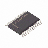
DS3881E+T&R/C Maxim Integrated Products, DS3881E+T&R/C Datasheet - Page 7

DS3881E+T&R/C
Manufacturer Part Number
DS3881E+T&R/C
Description
IC AUTO CCFL CTRLR 1CH 24-TSSOP
Manufacturer
Maxim Integrated Products
Type
CCFL Controllerr
Datasheet
1.DS3881EC.pdf
(28 pages)
Specifications of DS3881E+T&R/C
Frequency
40 ~ 100 kHz
Current - Supply
12mA
Voltage - Supply
4.75 V ~ 5.25 V
Operating Temperature
-40°C ~ 105°C
Package / Case
24-TSSOP
Lead Free Status / RoHS Status
Lead free / RoHS Compliant
Current - Output
-
Lead Free Status / Rohs Status
Details
13, 21
22, 23
PIN
1, 9
10
11
12
14
15
16
17
18
19
20
24
2
3
4
5
6
7
8
Single-Channel Automotive CCFL Controller
GA1, GB1 MOSFET A and B Gate Drive. Connect directly to logic-level mode n-channel MOSFET.
BRIGHT
PSYNC
GND_S
LSYNC
A0, A1
FAULT
NAME
POSC
SVMH
LOSC
SVML
LCM1
OVD1
STEP
GND
LCO
PDN
SDA
N.C.
SCL
V
CC
Address Select Input. Determines I
S er i al D ata Inp ut / O utp ut. I
Serial Clock Input. I
Lamp Frequency Input/Output. This pin is the input for an externally sourced lamp frequency
when the DS3881 is configured as a lamp frequency receiver. If the DS3881 is configured as a lamp
frequency source (i.e., the lamp frequency is generated internally), the frequency is output on this pin for
use by other lamp frequency receiver DS3881s.
Lam p Osci l l ator Resi stor Ad j ust. A r esi stor to g r ound on thi s l ead sets the fr eq uency of the i nter nal l am p osci l l ator .
Analog Brightness Control Input. Used to control the DPWM dimming feature. Ground if unused.
D P W M Inp ut/Outp ut. Thi s p i n i s the i np ut for an exter nal l y g ener ated D P WM si g nal w hen the D S 3881 i s
confi g ur ed as a D P WM r ecei ver . If the D S 3881 i s confi g ur ed as a D P WM sour ce ( i .e., the D P WM si g nal i s
g ener ated i nter nal l y) , the D P WM si g nal i s outp ut on thi s p i n for use b y other D P WM r ecei ver D S 3881s.
DPWM Oscillator Resistor Adjust. A resistor to ground on this lead sets the frequency of the DPWM
oscillator. This lead can optionally accept a 22.5Hz to 440Hz clock that will become the source timing of
the internal DPWM signal.
I
Low-Supply Voltage Monitor Input. Used to monitor the inverter voltage for undervoltage conditions.
High-Supply Voltage Monitor Input. Used to monitor the inverter voltage for overvoltage conditions.
Power Supply Connections. Both pins must be connected.
Lamp Current Monitor Input. Lamp current is monitored by a resistor placed in series with the low voltage
side of the lamp.
Overvoltage Detection. Lamp voltage is monitored by a capacitor divider placed on the high voltage side
of the transformer.
No Connection. Do not connect any signal to this pin.
Lamp Frequency Step Input. This active-high digital input moves the lamp oscillator frequency up or down
by either 1%, 2%, 3%, or 4% as configured in the EMIC register. This pin is logically ORed with the STEPE
bit in the EMIC register.
Ground Connection
Lamp Current Overdrive Enable Input. A high digital level at this input enables the lamp current overdrive
circuit. The amount of overdrive current is configured by the LCOC register. When this input is low, the
lamp current is set to its nominal level. This pin is logically ORed with the LCOE bit in the LCOC register.
Lamp On/Off Control Input. A low digital level at this input turns the lamp on. A high digital level clears the
fault logic, turns the lamp off, and places the device into the power-down mode. This pin is logically ORed
with the PDNE bit in the CR2 register.
Active-Low Fault Output. This open-drain pin requires external pullup resistor to realize high-logic levels.
2
C Interface Ground Connection. GND_S must be at the same potential as GND.
_____________________________________________________________________
2
C clock input.
2
C b i d i r ecti onal d ata p i n, w hi ch r eq ui r es a p ul l up r esi stor to r eal i ze hi g h l og i c l evel s.
2
C slave address.
FUNCTION
Pin Description
7


