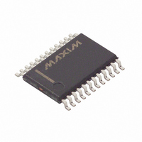
DS3881E+T&R/C Maxim Integrated Products, DS3881E+T&R/C Datasheet - Page 25

DS3881E+T&R/C
Manufacturer Part Number
DS3881E+T&R/C
Description
IC AUTO CCFL CTRLR 1CH 24-TSSOP
Manufacturer
Maxim Integrated Products
Type
CCFL Controllerr
Datasheet
1.DS3881EC.pdf
(28 pages)
Specifications of DS3881E+T&R/C
Frequency
40 ~ 100 kHz
Current - Supply
12mA
Voltage - Supply
4.75 V ~ 5.25 V
Operating Temperature
-40°C ~ 105°C
Package / Case
24-TSSOP
Lead Free Status / RoHS Status
Lead free / RoHS Compliant
Current - Output
-
Lead Free Status / Rohs Status
Details
Byte Read: A byte read is an 8-bit information transfer
from the slave to the master plus a 1-bit ACK or NACK
from the master to the slave. The 8 bits of information
that are transferred (most significant bit first) from the
slave to the master are read by the master using the bit
read definition above, and the master transmits an ACK
using the bit write definition to receive additional data
bytes. The master must NACK the last byte read to ter-
minate communication so the slave will return control of
SDA to the master.
Slave Address Byte: Each slave on the I
responds to a slave addressing byte sent immediately
following a start condition. The slave address byte
(Figure 10) contains the slave address in the most sig-
nificant seven bits and the R/W bit in the least signifi-
cant bit. The DS3881’s slave address is 10100A
(binary), where A
pins (A0 and A1). The address pin allows the device to
respond to one of four possible slave addresses. By
writing the correct slave address with R/W = 0, the
master indicates it will write data to the slave. If R/W =
1, the master will read data from the slave. If an incor-
rect slave address is written, the DS3881 will assume
the master is communicating with another I
and ignore the communications until the next start con-
dition is sent.
Memory Address: During an I
master must transmit a memory address to identify the
memory location where the slave is to store the data.
The memory address is always the second byte trans-
mitted during a write operation following the slave
address byte.
Writing a Data Byte to a Slave: The master must gen-
erate a start condition, write the slave address byte
(R/W = 0), write the memory address, write the byte of
data, and generate a stop condition. Remember the
master must read the slave’s acknowledgement during
all byte write operations. See Figure 11 for more detail.
Single-Channel Automotive CCFL Controller
0
and A
1
are the values of the address
2
C write operation, the
I
2
C Communication
____________________________________________________________________
2
C device
2
C bus
1
A
0
0
Acknowledge Polling: Any time EEPROM is written,
the DS3881 requires the EEPROM write time (t
the stop condition to write the contents to EEPROM.
During the EEPROM write time, the DS3881 will not
acknowledge its slave address because it is busy. It is
possible to take advantage of that phenomenon by
repeatedly addressing the DS3881, which allows the
next byte of data to be written as soon as the DS3881 is
ready to receive the data. The alternative to acknowl-
edge polling is to wait for a maximum period of t
elapse before attempting to write again to the DS3881.
EEPROM Write Cycles: The number of times the
DS3881’s EEPROM can be written before it fails is
specified in the Nonvolatile Memory Characteristics
table. This specification is shown at the worst-case
write temperature. The DS3881 is typically capable of
handling many additional write cycles when the writes
are performed at room temperature.
Reading a Data Byte from a Slave: To read a single
byte from the slave the master generates a start condi-
tion, writes the slave address byte with R/W = 0, writes
the memory address, generates a repeated start condi-
tion, writes the slave address with R/W = 1, reads the
data byte with a NACK to indicate the end of the trans-
fer, and generates a stop condition. See Figure 11 for
more detail.
Figure 10. DS3881’s Slave Address Byte
SIGNIFICANT BIT
MOST
1
7-BIT SLAVE ADDRESS
0
1
0
A
1,
A
0 A
0
PIN VALUE
1
A
0
R/W
READ OR WRITE
DETERMINES
W
) after
W
25
to


