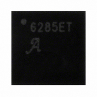
A6285EET-T Allegro Microsystems Inc, A6285EET-T Datasheet - Page 8

A6285EET-T
Manufacturer Part Number
A6285EET-T
Description
IC LED DRIVER LINEAR 32-QFN
Manufacturer
Allegro Microsystems Inc
Type
Linear (Non-Switching)r
Datasheet
1.A6285EET-T.pdf
(13 pages)
Specifications of A6285EET-T
Operating Temperature
-40°C ~ 85°C
Topology
PWM
Constant Current
Yes
Number Of Outputs
16
Internal Driver
Yes
Type - Primary
Backlight
Type - Secondary
Color, White LED
Frequency
30MHz
Voltage - Supply
3 V ~ 5.5 V
Voltage - Output
12V
Mounting Type
Surface Mount
Package / Case
32-VFQFN Exposed Pad
Current - Output / Channel
80mA
Internal Switch(s)
Yes
Led Driver Application
Display
No. Of Outputs
16
Output Current
80mA
Output Voltage
12V
Input Voltage
3V To 5.5V
Dimming Control Type
PWM
Lead Free Status / RoHS Status
Lead free / RoHS Compliant
Efficiency
-
Lead Free Status / RoHS Status
Lead free / RoHS Compliant
Other names
620-1224-5
A6285
Setting Maximum Channel Current The maximum output
current per channel is set by a single external resistor, REXT,
which is placed between the REXT pin and PGND. The voltage
on REXT, V
channel current is equivalent to the current flowing through
REXT multiplied by 38.4. The maximum channel output current
can be calculated as:
where:
Figure 4 shows the maximum per channel constant output cur-
rent, I
resistor between REXT terminal and ground.
Dot Correction The A6285 can independently fine-adjust
the current of each output channel, a feature referred to as dot
correction. This feature is used to compensate for the brightness
deviations of the LEDs connected to the output channels, OUT0
through OUT15.
Each of the 16 channels can be programmed with a 7-bit word.
The channel output can be adjusted in 128 steps from 0% to
100% of the maximum programmable per channel output cur-
rent, I
OUTx:
where DC
for each output channel.
Dot correction data is entered for all channels at the same time.
The complete dot correction data format consists of sixteen 7-bit
words, which form a 112-bit (16 × 7) wide serial data packet. The
data for each channel is sent in a continuous sequence, and all
data is clocked in with the MSB first, as shown in figure 7.
To input data into the Dot Correction register, LE should be set
low, and MODE must be set high. MODE sets the input shift reg-
ister to 112-bit width. After all serial data is clocked in, a rising
edge on the LE terminal latches the data into the Dot Correction
V
R
should not be less than 600 Ω, corresponding to 80 mA.
EXT
EXT
O
O
(max), of OUT0 to OUT15, versus R
(max). Equation 2 determines the output current for each
is the value of the user-selected external resistor, which
is 1.25 V typical, and
x
is the programmed dot-correction value (0, 1, …127)
EXT
, is set by an internal band gap. The maximum
I
I
O
Ox
(max) =
=
I
O
(max) × DC
V
R
127
EXT
EXT
×
38.4 ,
16-Channel Constant-Current Latched LED Driver
x
,
EXT
,
, the value of the
with Open LED Detection and Dot Correction
Functional Description
(1)
(2)
register. The timing sequence is shown in figure 9.
All Channel Output Enable-Disable All OUTx channels
of the A6285 can switched off using the O ¯ ¯ E ¯ pin. When O ¯ ¯ E ¯ is
set high, all OUTx outputs are disabled, regardless of the on/off
status of any OUTx. When O ¯ ¯ E ¯ is set to low, the on/off status of
each OUTx is determined by the state of the latches in the On/Off
register. O ¯ ¯ E ¯ can be PWMed to control the average current, which
controls the LED brightness of all outputs, in addition to the DC
function.
Individual Channel Output Enable-Disable Each OUTx
channel can be switched on or off independently. Each of the
channels can be programmed with a 1-bit word.
On/off data is entered for all channels at the same time. The
complete on/off data format consists of sixteen 1-bit words, which
form a 16-bit wide serial data packet. The data for each channel is
sent in a continuous sequence, and all data is clocked in with the
MSB first, as shown in figure 8.
To input data into the On/Off register, LE must be set low, and
MODE must be set low. LE allows on/off data to enter the input
shift register, and MODE sets the input shift register to 16-bit
width. After all serial data is clocked in, a rising edge on the LE
terminal latches the data into the On/Off register and moves the
LOD data at the Open Circuit Detector into the input shift regis-
ter. The timing sequence is shown in figure 9.
Figure 7. Dot Correction (DC) data format
Figure 8. Individual output on-off data format
DC 0.0
LSB
0
DC
…
OUT0
DC 0.6
On/Off
OUT
LSB
6
0
0
DC 1.0
On/Off
DC
7
1
OUT2
OUT
115 Northeast Cutoff
1.508.853.5000; www.allegromicro.com
Allegro MicroSystems, Inc.
Worcester, Massachusetts 01615-0036 U.S.A.
1
…
through DC
through OUT
…
OUT14
DC 14.6
14
104
On/Off
14
DC 15.0
On/Off
OUT
105
MSB
15
15
DC
…
OUT15
DC 15.6
MSB
111
8


