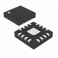
MAX7302ATE+T Maxim Integrated Products, MAX7302ATE+T Datasheet - Page 12

MAX7302ATE+T
Manufacturer Part Number
MAX7302ATE+T
Description
IC LED DRIVER LINEAR 16-TQFN
Manufacturer
Maxim Integrated Products
Type
Linear (I²C Interface)r
Datasheet
1.MAX7302AEE.pdf
(30 pages)
Specifications of MAX7302ATE+T
Topology
Open Drain, PWM
Number Of Outputs
9
Internal Driver
Yes
Type - Primary
Backlight, LED Blinker
Type - Secondary
White LED
Frequency
1MHz
Voltage - Supply
1.62 V ~ 3.6 V
Mounting Type
Surface Mount
Package / Case
16-TQFN Exposed Pad
Operating Temperature
-40°C ~ 125°C
Current - Output / Channel
25mA
Internal Switch(s)
Yes
Lead Free Status / RoHS Status
Lead free / RoHS Compliant
Voltage - Output
-
Efficiency
-
Lead Free Status / Rohs Status
Details
Ports P2–P9 are overvoltage protected to V
even for a port used as an input with a V
input threshold. Port P1 is overvoltage protected to 5.5V,
independent of V
outputs with more than one voltage swing on a group of
ports using the same port supply, set the port supply volt-
age (V
outputs and port P1 for the highest voltage ports, and use
open-drain outputs with external pullup resistors for the
lower voltage ports. When P2–P9 are acting as inputs ref-
erenced to V
than V
Use the port lock registers to lock any combination of
port I/O register functionality (see Table 8). The port
lock registers are unlocked on power-up or by configur-
ing the RSTPOR bit to reset to POR value. The bits in
the port lock register can only be written to once. After
setting a bit to logic-high, the bit can only be cleared
by powering off the device.
SMBus/I
Level-Translating GPIO and LED Driver with CLA
Figure 2. Output Port Structure
Figure 3. Port I/O Structure
12
______________________________________________________________________________________
DD
LA
) to be the highest output voltage. Use push-pull
- 0.3V.
CLOCK
DD
, make sure the V
DD
OUTPUT
SELECT
2
INPUT
and V
C Interfaced 9-Port,
LA
V+
(see Figure 3). To mix logic
3-BIT PRESCALER
P1
CONFIG26 [4:2]
V
LA
Port Lock Registers
LA
voltage is greater
LA
DD
. This is true
port logic-
PORT P1
PORT_ [4:0]
4-BIT BLINK
PORT_ [3:0]
5-BIT PWM
When a bit position in the port lock register is set, the
corresponding port I/O registers cannot change. When a
port I/O register is locked as an output, none of its output
register settings can change. When a port I/O register is
locked as an input, only bits D0 and D1 can change, and
the locked input behaviour options, such as debounce
and transition detection, operate as normal.
The MAX7302 samples the input ports every 31ms if
input debouncing is enabled for an input port (D2 = 1
of the port I/O register). The MAX7302 compares each
new sample with the previous sample. If the new sam-
ple and the previous sample have the same value, the
corresponding internal register updates.
When the port input is read through the serial interface,
the MAX7302 does not return the instantaneous value
of the logic level from the port because debounce is
active. Instead, the MAX7302 returns the stored
debounced input signal.
PORT_ [5]
OUTPUT
SELECT
INPUT
V+
P2–P9
0
1
V
LA
I/O
P2–P9
PORT
Input Debounce


