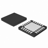
NCP5680MUTXG ON Semiconductor, NCP5680MUTXG Datasheet - Page 22

NCP5680MUTXG
Manufacturer Part Number
NCP5680MUTXG
Description
IC LED DRIVER WHT HI EFF 24-UQFN
Manufacturer
ON Semiconductor
Type
Photo Flash LED (I²C Interface)r
Datasheet
1.NCP5680MUTXG.pdf
(27 pages)
Specifications of NCP5680MUTXG
Topology
Switched Capacitor (Charge Pump)
Number Of Outputs
2
Internal Driver
No
Type - Primary
Flash/Torch
Type - Secondary
White LED
Frequency
850kHz ~ 1.15MHz
Voltage - Supply
2.7 V ~ 5.5 V
Voltage - Output
4.5 V ~ 5.3 V
Mounting Type
Surface Mount
Package / Case
24-UFQFN Exposed Pad, 24-UFQFN
Operating Temperature
-40°C ~ 85°C
Current - Output / Channel
400mA
Internal Switch(s)
Yes
Lead Free Status / RoHS Status
Lead free / RoHS Compliant
Efficiency
-
Lead Free Status / Rohs Status
Details
Available stocks
Company
Part Number
Manufacturer
Quantity
Price
Company:
Part Number:
NCP5680MUTXG
Manufacturer:
ON Semiconductor
Quantity:
2 050
the 200 ms time out can be activated by forcing the TPLGT
bit to high in the CONFIG0 register. The Picture Light
cannot be combined with a power flash pulse.
NTC Sensor
in the CONFIG0 register. When the function is activated,
the external NTC element is biased by a programmable
constant current (in the 10 mA to 630 mA range), the voltage
developed across the NTC pin and GND being compared
to the reference voltage stored into the NTCREG register.
When the NTC voltage drops below the minimum level
(setup by the NTCREG register), the charge is de−activated
and both the flash and the torch mode are automatically
switched OFF, reducing the power dissipated into the LED
to almost zero. The associated flip flop is reset to the
normal mode when a power OFF/ON sequence is forced,
applied to the external NMOS transistor: this signal is fully
synchronized with a photo flash pulse. The positive going
slope generates a negative pulse at the RESET input of the
flip flop built with two NAND gate which, in turn, activates
the delay built with the RC network connected to a single
inverter. The flip−flop is set when the RC timing ends (a
negative going pulse is present at the SET input), turning
ON the external NMOS transistor which, in turn, will force
to ground the gate of the power transistor. At this point, the
ILED current is disconnected and no more power is
dissipated in the circuit. To flip flop is reset by sending a
The external NTC element is controlled by the ENTC bit
The NMOS signal is derived from the gate drive voltage
Implementation = NMOS
Implementation = /POR
S1
S1
DSTM1
DSTM2
C1
1n
100k
Figure 21. Basic External Hardware Time Out Security Circuit
R1
12
13
74HC132
U4D
11
http://onsemi.com
Run
V
1
2
22
74HC08
TimeMax
U3A
or by pulsed Hi/Lo the NTCREG[CNTC] bit. In both case,
the NTC temperature must be cool enough to enable the
power current flow into the LED.
Time Out Security
application, and external structure shall be implemented to
handle the worst but rare case condition, i.e. when the
NCP5680 built−in timer and time out fail simultaneously.
To handle such conditions, an external circuit will switch
off the two NMOS transistor when the time extend the
maximum 200 ms time out defined by the passive
component. There is no software associated with the
security circuit, the activation being automatically done
when any of the two NMOS is used to generate a power
flash pulse. The typical circuit is depicted in Figure 21.
new photo flash sequence, or using any kind of MCU
controlled signal.
I2C Protocol
possibility to take control of the bus, programmed by
means of the standard I2C protocol driven by the external
MCU. In addition, the internal STATUS register can be
read back upon request coming from the external MCU.
takes place with three serial bytes:
V
When an extra security is requested by the end
The NCP5680 is considered as a Slave system, with no
To program one particular register, the communication
8
74HC132
3
U4C
4
5
2
1
74HC132
74HC132
U4B
U4A
9
10
3
6
R2
1000k
C2
100n
Time−Out
D1
D1N4148
V


