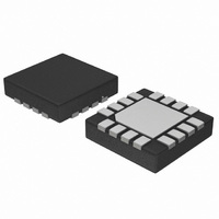
NCP5604BMTR2G ON Semiconductor, NCP5604BMTR2G Datasheet - Page 8

NCP5604BMTR2G
Manufacturer Part Number
NCP5604BMTR2G
Description
IC DRIVER LED WHITE HE 16-QFN
Manufacturer
ON Semiconductor
Type
Backlight, White LEDr
Datasheet
1.NCP5604AMTR2G.pdf
(15 pages)
Specifications of NCP5604BMTR2G
Topology
PWM, Switched Capacitor (Charge Pump)
Number Of Outputs
4
Internal Driver
Yes
Type - Primary
Backlight, Flash/Torch
Type - Secondary
White LED
Frequency
850kHz ~ 1.15MHz
Voltage - Supply
2.7 V ~ 5.5 V
Voltage - Output
4.8 V ~ 6 V
Mounting Type
Surface Mount
Package / Case
16-TFQFN Exposed Pad
Operating Temperature
-40°C ~ 85°C
Current - Output / Channel
100mA
Internal Switch(s)
Yes
Efficiency
85%
Number Of Segments
3
Operating Supply Voltage
2.7 V to 5.5 V
Maximum Supply Current
1 mA
Maximum Power Dissipation
320 mW
Maximum Operating Temperature
+ 85 C
Mounting Style
SMD/SMT
Minimum Operating Temperature
- 40 C
Lead Free Status / RoHS Status
Lead free / RoHS Compliant
Other names
NCP5604BMTR2G
NCP5604BMTR2GOSTR
NCP5604BMTR2GOSTR
Available stocks
Company
Part Number
Manufacturer
Quantity
Price
Part Number:
NCP5604BMTR2G
Manufacturer:
ON/安森美
Quantity:
20 000
11. The overall output current tolerance depends upon the accuracy of the external resistor. Using 1% or better resistor is recommended.
12. The external circuit must not force the I
DC-DC OPERATION
generate a DC voltage capable to supply the White LED
load The system regulates the current flowing into each
LED by means of internal current mirrors associated with
the white diodes. Consequently, the output voltage will be
equal to the Vf of the LED, plus the 300 mV (typical)
developed across the internal NMOS mirror. Typically,
assuming a standard white LED forward biased at 10 mA,
the output voltage will be 3.8 V.
extra mode of operation, with a significant efficiency
improvement of the converter over the normal battery
voltage span. The threshold levels have been defined to
optimize this range of operating voltage, assuming a high
efficiency is not relevant when the system is connected to
a battery charger ( i.e. Vbat > 4.5 V).
output and stops the converter when the voltage is above
5.0 V. The converter resumes to normal operation when the
voltage drops below 5.0 V (no latch-up mechanism).
Consequently, the chip can operate with no load during any
test procedures, but in the case of special applications, it is
recommended to connect the non used LED driver either to
a LED, or to the Vbat supply to minimize the internal losses
(see LOAD CONNECTION paragraph).
LOAD CURRENT CALCULATION
voltage provided by the internal Band Gap associated to the
external resistor connected across I
Figure 4). In any case, no voltage shall be forced at I
pin, either downward or upward.
k = 260 to yield the output load current. Since the reference
ANALOG SECTION
temperature, operating conditions 2.85 V < Vbat < 5.5 V, unless otherwise noted.)
DIGITAL PARAMETERS SECTION
ambient temperature, operating conditions 2.85 V < Vbat < 5.5 V, unless otherwise noted.) Note: Digital inputs undershoot < - 0.30 V to
ground, Digital inputs overshoot < 0.30 V to V
The converter is based on a charge pump technique to
The third external capacitor makes possible the 1.33X
The built-in OVP circuit continuously monitor each
The load current is derived from the 600 mV reference
The reference current is multiplied by the constant
Pin
Pin
3
3
-
2
2
2
Symbol
Symbol
F
I
V
I
LEDR
REF
PWM
V
V
REF
IH
IL
(Typical values are referenced to T
Reference Current @ Vref = 600 mV (Note 11)
Reference Voltage (Note 12)
Reference Current (IREF) to Output LED Current Ratio
Input Enable PWM
Positive Going Input High Voltage Threshold, EN Signal
Negative Going Input High Voltage Threshold, EN Signal
REF
REF
(Typical values are referenced to T
pin and Ground (see
BAT
pin voltage either higher or lower than the 600 mV specified.
.
APPLICATIONS INFORMATION
NCP5604A, NCP5604B
Rating
Rating
http://onsemi.com
A
= +25°C, Min & Max values are referenced -40°C to +85°C ambient
REF
8
voltage is based on a temperature compensated Band Gap
structure, a tight tolerance resistor will provide a very
accurate load current. The resistor is calculated from the
Ohm's law (R
equation can be arranged to define the resistor value for a
given output current:
R
312 kW. Obviously, the tolerance of such a resistor must be
1% or better, with a 100 ppm thermal coefficient, to get the
expected overall tolerance.
GND
bias
Consequently, the resistor value will range between
A
= +25°C, Min & Max values are referenced -40°C to +85°C
I
REF
= 156/25 mA = 6240 W and R
Figure 4. Basic Reference Current Source
Pin 3
bias
VBandGap
R bias + (Vref * k) Iout
R bias + (0.6 * 260) Iout
+
-
Note: The I
to voltage higher than 600 mV.
R bias + 156 Iout
= Vref/I
-2%
Min
Min
1.0
0.1
1.3
-
0
600mV
REF
REF
Typ
Typ
600
260
pin must never be biased
) and a more practical
-
-
-
-
GND
bias
= 156/0.5 mA =
V
Max
+2%
Max
100
200
0.4
BAT
-
LED Return
Pin 5 to 8
Unit
Unit
kHz
mV
mA
(eq. 1)
(eq. 2)
V
V
-


