NCP5604BMTR2G ON Semiconductor, NCP5604BMTR2G Datasheet - Page 5
NCP5604BMTR2G
Manufacturer Part Number
NCP5604BMTR2G
Description
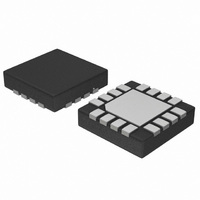
IC DRIVER LED WHITE HE 16-QFN
Manufacturer
ON Semiconductor
Type
Backlight, White LEDr
Datasheet
1.NCP5604AMTR2G.pdf
(15 pages)
Specifications of NCP5604BMTR2G
Topology
PWM, Switched Capacitor (Charge Pump)
Number Of Outputs
4
Internal Driver
Yes
Type - Primary
Backlight, Flash/Torch
Type - Secondary
White LED
Frequency
850kHz ~ 1.15MHz
Voltage - Supply
2.7 V ~ 5.5 V
Voltage - Output
4.8 V ~ 6 V
Mounting Type
Surface Mount
Package / Case
16-TFQFN Exposed Pad
Operating Temperature
-40°C ~ 85°C
Current - Output / Channel
100mA
Internal Switch(s)
Yes
Efficiency
85%
Number Of Segments
3
Operating Supply Voltage
2.7 V to 5.5 V
Maximum Supply Current
1 mA
Maximum Power Dissipation
320 mW
Maximum Operating Temperature
+ 85 C
Mounting Style
SMD/SMT
Minimum Operating Temperature
- 40 C
Lead Free Status / RoHS Status
Lead free / RoHS Compliant
Other names
NCP5604BMTR2G
NCP5604BMTR2GOSTR
NCP5604BMTR2GOSTR
Available stocks
Company
Part Number
Manufacturer
Quantity
Price

Part Number:
NCP5604BMTR2G
Manufacturer:
ON/安森美
Quantity:
20 000


1. Using low ESR 1.0 mF ceramic capacitor is mandatory to optimize the Charge Pump efficiency. The DC Bias effect must be taken into account
2. Total DC-DC output current is limited to 100 mA.
3. The exposed flag shall be connected to ground.
PIN FUNCTION DESCRIPTION
Pin
when selecting the ceramic capacitor. Smallest foot print packages (size 0602 and lower) are prone to strong DC bias effect, reducing the real
capacitance significantly.
10
11
12
13
14
15
16
1
2
3
4
5
6
7
8
9
Symbol
AGND
PGND
VOUT
VBAT
LED4
LED3
LED2
LED1
C1N
C1P
C2P
C2N
C3P
C3N
I
EN
REF
OUTPUT, POWER
INPUT, ANALOG
INPUT, POWER
INPUT, DIGITAL
INPUT, POWER
INPUT, POWER
INPUT, POWER
INPUT, POWER
POWER
POWER
POWER
POWER
POWER
POWER
POWER
POWER
Type
Input Battery voltage to supply the analog and digital blocks. The pin must be decoupled to
ground by a 1.0 mF ceramic capacitor.
This pin carries the Enable function to control the DC-DC converter. It can be used to
digitally dim the LED by using a PWM technique.
The digital PWM dimming can operate over the 100 Hz - 200 kHz frequency, depending
upon the application requirements.
This pin provides the reference current, based on the internal bandgap voltage reference,
to control the output current flowing in the LED. A 1% tolerance, or better, resistor shall be
used to get the highest accuracy of the LED biases. An external current source can be
used to bias this pin to dim the light coming out of the LED.
In no case shall the voltage at pin 3 be forced either higher or lower than the 600 mV
provided by the internal reference.
This pin is the GROUND signal for the analog and digital blocks and must be connected to
the system ground.
NCP5604A: This pin sinks to ground and monitors the current flowing into the fourth LED,
intended to be used in backlight application. The current is limited to 25 mA maximum
(Note 2).
NCP5604B: This pin is not connected.
This pin sinks to ground and monitors the current flowing into the third LED, intended to be
used in backlight application. The current is limited to 25 mA maximum (Note 2).
This pin sinks to ground and monitors the current flowing into the second LED, intended to
be used in backlight application. The current is limited to 25mA maximum (Note 2).
This pin sinks to ground and monitors the current flowing into the first LED, intended to be
used in backlight application. The current is limited to 25 mA maximum (Note 2).
This pin is the GROUND reference for the DC-DC converter and the output current
control. The pin must be connected to the system ground, a ground plane being strongly
recommended.
One side of the external charge pump capacitor (C
with C1P, pin 11 (Note 1).
One side of the external charge pump capacitor (C
with C1N, pin 10 (Note 1).
This pin provides the output voltage supplied by the DC-DC converter. The Vout pin must
be bypassed by 1.0 mF ceramic capacitor located as close as possible to the pin to
properly bypass the output voltage to ground. The circuit shall not operate without such
bypass capacitor properly connected to the Vout pin.
The output voltage is internally clamped to 5.5 V in the event of no load situation. On the
other hand, the output current is limited to 100 mA in the event of a short circuit to ground.
One side of the external charge pump capacitor (C
with C2N, pin 14 (Note 1).
One side of the external charge pump capacitor (C
with C2P, pin 13 (Note 1).
One side of the external charge pump capacitor (C
with C3N, pin 16 (Note 1).
One side of the external charge pump capacitor (C
with C3P, pin 15 (Note 1).
EN = Low ³ shutdown mode, the DC-DC is disconnected from the load.
EN = High ³ operating mode, the DC-DC is activated.
NCP5604A, NCP5604B
http://onsemi.com
5
Description
FLY
FLY
FLY
FLY
FLY
FLY
) is connected to this pin, associated
) is connected to this pin, associated
) is connected to this pin, associated
) is connected to this pin, associated
) is connected to this pin, associated
) is connected to this pin, associated
Related parts for NCP5604BMTR2G
Image
Part Number
Description
Manufacturer
Datasheet
Request
R

Part Number:
Description:
High Efficiency White LED Driver
Manufacturer:
ON Semiconductor
Datasheet:
Part Number:
Description:
Current Mode Charge Pump Led Driver
Manufacturer:
ON Semiconductor
Datasheet:
Part Number:
Description:
ON Semiconductor [VOLTAGE REGULATOR]
Manufacturer:
ON Semiconductor
Datasheet:
Part Number:
Description:
357-036-542-201 CARDEDGE 36POS DL .156 BLK LOPRO
Manufacturer:
ON Semiconductor
Datasheet:
Part Number:
Description:
357-036-542-201 CARDEDGE 36POS DL .156 BLK LOPRO
Manufacturer:
ON Semiconductor
Datasheet:
Part Number:
Description:
357-036-542-201 CARDEDGE 36POS DL .156 BLK LOPRO
Manufacturer:
ON Semiconductor
Datasheet:
Part Number:
Description:
357-036-542-201 CARDEDGE 36POS DL .156 BLK LOPRO
Manufacturer:
ON Semiconductor
Datasheet:
Part Number:
Description:
357-036-542-201 CARDEDGE 36POS DL .156 BLK LOPRO
Manufacturer:
ON Semiconductor
Datasheet:
Part Number:
Description:
357-036-542-201 CARDEDGE 36POS DL .156 BLK LOPRO
Manufacturer:
ON Semiconductor
Datasheet:
Part Number:
Description:
357-036-542-201 CARDEDGE 36POS DL .156 BLK LOPRO
Manufacturer:
ON Semiconductor
Datasheet:
Part Number:
Description:
357-036-542-201 CARDEDGE 36POS DL .156 BLK LOPRO
Manufacturer:
ON Semiconductor
Datasheet:
Part Number:
Description:
357-036-542-201 CARDEDGE 36POS DL .156 BLK LOPRO
Manufacturer:
ON Semiconductor
Datasheet:
Part Number:
Description:
357-036-542-201 CARDEDGE 36POS DL .156 BLK LOPRO
Manufacturer:
ON Semiconductor
Datasheet:
Part Number:
Description:
Manufacturer:
ON Semiconductor
Datasheet: