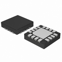
NCP5604BMTR2G ON Semiconductor, NCP5604BMTR2G Datasheet - Page 10

NCP5604BMTR2G
Manufacturer Part Number
NCP5604BMTR2G
Description
IC DRIVER LED WHITE HE 16-QFN
Manufacturer
ON Semiconductor
Type
Backlight, White LEDr
Datasheet
1.NCP5604AMTR2G.pdf
(15 pages)
Specifications of NCP5604BMTR2G
Topology
PWM, Switched Capacitor (Charge Pump)
Number Of Outputs
4
Internal Driver
Yes
Type - Primary
Backlight, Flash/Torch
Type - Secondary
White LED
Frequency
850kHz ~ 1.15MHz
Voltage - Supply
2.7 V ~ 5.5 V
Voltage - Output
4.8 V ~ 6 V
Mounting Type
Surface Mount
Package / Case
16-TFQFN Exposed Pad
Operating Temperature
-40°C ~ 85°C
Current - Output / Channel
100mA
Internal Switch(s)
Yes
Efficiency
85%
Number Of Segments
3
Operating Supply Voltage
2.7 V to 5.5 V
Maximum Supply Current
1 mA
Maximum Power Dissipation
320 mW
Maximum Operating Temperature
+ 85 C
Mounting Style
SMD/SMT
Minimum Operating Temperature
- 40 C
Lead Free Status / RoHS Status
Lead free / RoHS Compliant
Other names
NCP5604BMTR2G
NCP5604BMTR2GOSTR
NCP5604BMTR2GOSTR
Available stocks
Company
Part Number
Manufacturer
Quantity
Price
Part Number:
NCP5604BMTR2G
Manufacturer:
ON/安森美
Quantity:
20 000
Vout and ground, but the current through such network will
not be regulated by the NCP5604A chip (see Figure 10).
On top of that, the total current out of the Vout pin shall be
limited to 100 mA.
DIMMING
•
•
100% duty cycle, but the output current is pulsed since the
system is continuously switched ON/OFF. There is no need
for extra passive component, the clock being provided by
an I/O port from the MCU (see Figure 11).
GND
GND
CONTROL
Figure 9. Using the NCP5604B to Drive a Three LED
Finally, an external network can be connected across
The dimming can be achieved by two means:
The digital PWM is straightforward, yielding a zero to
Use a digital PWM signal to control the EN pin
Use an analog signal to control the reference current
IREF pin.
4.7uF/6.3V
Figure 10. Extra Load Connected to Vout
GND
C4
12
8
7
6
5
100k
R1
Vbat
C5
1
2
3
4
9
VBAT
EN
IREF
AGND
PGND
1 mF/6.3 V
U1
NCP5604B
220 nF/10 V
Layout
C3
D3
VOUT
C2N
C1N
C2P
C1P
LWY87S
D2
LWY87S
14
13
11
10
12
LWY87S
D1
NCP5604A, NCP5604B
220 nF/10 V
220 nF/10 V
C2
C1
GND
http://onsemi.com
C5
GND
10
circuit has been properly started. On the other hand, with
a 1% to 99% span, the circuit supports a large Duty Cycle
to accommodate any range of dimming. The waveforms
given in Figure 12 illustrate the NCP5604A behavior
during the 50 kHz PWM operation. The same mechanism
applies for the NCP5604B version.
technique can be built with two extra components (one
resistor + one NMOS), the net advantage being a
continuous output current once the operating point has
been stabilized (see Figure 13). The absolute output
current tolerance depends upon the precision of the two
external resistors, the R
negligible in front of the resistor value. The example given,
Figure 13 yields a 1.0 mA output current when Q1 is OFF,
Input PWM Signal Frequency:
100 Hz to 200 kHz
The PWM frequency can be up to 200 kHz once the
Besides the popular PWM mode, a simple analog
Figure 11. Basic Digital PWM Dimming Control
Figure 12. PWM Modulation Span: 1% to 99%
PWM
GND
GND
DS(on)
1
2 2
3
4
9
VBAT
EN
IREF
AGND
PGND
of the NMOS being
VOUT
C2N
C3N
C2P
C3P


