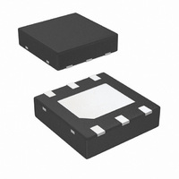
LM3410XSD/NOPB National Semiconductor, LM3410XSD/NOPB Datasheet - Page 3

LM3410XSD/NOPB
Manufacturer Part Number
LM3410XSD/NOPB
Description
IC LED DRVR WT/OLED BCKLGT 6-LLP
Manufacturer
National Semiconductor
Series
PowerWise®r
Type
Backlight, OLED, White LEDr
Datasheet
1.LM3410XMFNOPB.pdf
(32 pages)
Specifications of LM3410XSD/NOPB
Constant Current
Yes
Topology
PWM, SEPIC, Step-Up (Boost)
Number Of Outputs
1
Internal Driver
Yes
Type - Primary
Automotive, Backlight, Flash/Torch
Type - Secondary
High Brightness LED (HBLED), OLED, White LED
Frequency
1.2MHz ~ 2MHz
Voltage - Supply
2.7 V ~ 5.5 V
Voltage - Output
3 V ~ 24 V
Mounting Type
Surface Mount
Package / Case
6-LLP
Operating Temperature
-40°C ~ 125°C
Current - Output / Channel
2.8A
Internal Switch(s)
Yes
Efficiency
88%
For Use With
LM3410XSDLEDEV - BOARD EVAL LM3410 BOOST LLP
Lead Free Status / RoHS Status
Lead free / RoHS Compliant
Other names
LM3410XSDTR
Pin Descriptions - 5-Pin SOT23
Pin Descriptions - 6-Pin LLP
Pin Descriptions - 8-Pin eMSOP
DAP
DAP
Pin
Pin
Pin
1
2
3
4
5
1
2
3
4
5
6
1
2
3
4
5
6
7
8
PGND
AGND
PGND
AGND
Name
Name
Name
GND
GND
GND
DIM
DIM
DIM
VIN
SW
VIN
VIN
SW
SW
FB
FB
FB
-
-
Function
No Connect
Power ground pin. Place PGND and output capacitor GND close together.
Supply voltage for power stage, and input supply voltage.
Dimming & shutdown control input. Logic high enables operation. Duty Cycle from 0 to 100%. Do not allow
this pin to float or be greater than VIN + 0.3V.
Feedback pin. Connect FB to external resistor divider to set output voltage.
Signal ground pin. Place the bottom resistor of the feedback network as close as possible to this pin & pin 5
Output switch. Connect to the inductor, output diode.
No Connect
Signal & Power ground. Connect to pin 2 & pin 6 on top layer. Place 4-6 vias from DAP to bottom layer GND
plane.
Function
Output switch. Connect to the inductor, output diode.
Signal and power ground pin. Place the bottom resistor of the feedback network as close as possible to this
pin.
Feedback pin. Connect FB to external resistor divider to set output voltage.
Dimming & shutdown control input. Logic high enables operation. Duty Cycle from 0 to 100%. Do not allow
this pin to float or be greater than VIN + 0.3V.
Supply voltage pin for power stage, and input supply voltage.
Function
Power ground pin. Place PGND and output capacitor GND close together.
Supply voltage for power stage, and input supply voltage.
Dimming & shutdown control input. Logic high enables operation. Duty Cycle from 0 to 100%. Do not allow
this pin to float or be greater than VIN + 0.3V.
Feedback pin. Connect FB to external resistor divider to set output voltage.
Signal ground pin. Place the bottom resistor of the feedback network as close as possible to this pin & pin
4.
Output switch. Connect to the inductor, output diode.
Signal & Power ground. Connect to pin 1 & pin 5 on top layer. Place 4-6 vias from DAP to bottom layer GND
plane.
3
www.national.com


