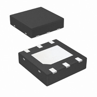
LM3410XSD/NOPB National Semiconductor, LM3410XSD/NOPB Datasheet - Page 17

LM3410XSD/NOPB
Manufacturer Part Number
LM3410XSD/NOPB
Description
IC LED DRVR WT/OLED BCKLGT 6-LLP
Manufacturer
National Semiconductor
Series
PowerWise®r
Type
Backlight, OLED, White LEDr
Datasheet
1.LM3410XMFNOPB.pdf
(32 pages)
Specifications of LM3410XSD/NOPB
Constant Current
Yes
Topology
PWM, SEPIC, Step-Up (Boost)
Number Of Outputs
1
Internal Driver
Yes
Type - Primary
Automotive, Backlight, Flash/Torch
Type - Secondary
High Brightness LED (HBLED), OLED, White LED
Frequency
1.2MHz ~ 2MHz
Voltage - Supply
2.7 V ~ 5.5 V
Voltage - Output
3 V ~ 24 V
Mounting Type
Surface Mount
Package / Case
6-LLP
Operating Temperature
-40°C ~ 125°C
Current - Output / Channel
2.8A
Internal Switch(s)
Yes
Efficiency
88%
For Use With
LM3410XSDLEDEV - BOARD EVAL LM3410 BOOST LLP
Lead Free Status / RoHS Status
Lead free / RoHS Compliant
Other names
LM3410XSDTR
analysis of the LM3410 Boost Converter is applicable to the
LM3410 SEPIC Converter.
SEPIC Design Guide:
SEPIC Conversion ratio without loss elements:
Therefore:
Small ripple approximation:
In a well-designed SEPIC converter, the output voltage, and
input voltage ripple, the inductor ripple I
comparison to the DC magnitude. Therefore it is a safe ap-
proximation to assume a DC value for these components. The
main objective of the Steady State Analysis is to determine
the steady state duty-cycle, voltage and current stresses on
all components, and proper values for all components.
In a steady-state converter, the net volt-seconds across an
inductor after one cycle will equal zero. Also, the charge into
a capacitor will equal the charge out of a capacitor in one cy-
cle.
Therefore:
Substituting I
L1
into I
L2
I
L2
= I
LED
FIGURE 14. HB/OLED SEPIC CONVERTER Schematic
L1
and I
L2
is small in
17
The average inductor current of L2 is the average output load.
Applying Charge balance on C1:
Since there are no DC voltages across either inductor, and
capacitor C3 is connected to Vin through L1 at one end, or to
ground through L2 on the other end, we can say that
Therefore:
This verifies the original conversion ratio equation.
It is important to remember that the internal switch current is
equal to I
so that the minimum guaranteed peak switch current limit
(2.1A) is not exceeded.
FIGURE 13. Inductor Volt-Sec Balance Waveform
L1
and I
L2
during the D interval. Design the converter
V
C3
= V
IN
30038552
www.national.com
30038556


