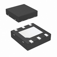
LM3410XSD/NOPB National Semiconductor, LM3410XSD/NOPB Datasheet - Page 10

LM3410XSD/NOPB
Manufacturer Part Number
LM3410XSD/NOPB
Description
IC LED DRVR WT/OLED BCKLGT 6-LLP
Manufacturer
National Semiconductor
Series
PowerWise®r
Type
Backlight, OLED, White LEDr
Datasheet
1.LM3410XMFNOPB.pdf
(32 pages)
Specifications of LM3410XSD/NOPB
Constant Current
Yes
Topology
PWM, SEPIC, Step-Up (Boost)
Number Of Outputs
1
Internal Driver
Yes
Type - Primary
Automotive, Backlight, Flash/Torch
Type - Secondary
High Brightness LED (HBLED), OLED, White LED
Frequency
1.2MHz ~ 2MHz
Voltage - Supply
2.7 V ~ 5.5 V
Voltage - Output
3 V ~ 24 V
Mounting Type
Surface Mount
Package / Case
6-LLP
Operating Temperature
-40°C ~ 125°C
Current - Output / Channel
2.8A
Internal Switch(s)
Yes
Efficiency
88%
For Use With
LM3410XSDLEDEV - BOARD EVAL LM3410 BOOST LLP
Lead Free Status / RoHS Status
Lead free / RoHS Compliant
Other names
LM3410XSDTR
www.national.com
age and the operating temperature. The ESL of an input
capacitor is usually determined by the effective cross sec-
tional area of the current path. At the operating frequencies
of the LM3410, certain capacitors may have an ESL so large
that the resulting impedance (2
required to provide stable operation. As a result, surface
mount capacitors are strongly recommended. Multilayer ce-
ramic capacitors (MLCC) are good choices for both input and
output capacitors and have very low ESL. For MLCCs it is
recommended to use X7R or X5R dielectrics. Consult capac-
itor manufacturer datasheet to see how rated capacitance
varies over operating conditions.
OUTPUT CAPACITOR
The LM3410 operates at frequencies allowing the use of ce-
ramic output capacitors without compromising transient re-
sponse. Ceramic capacitors allow higher inductor ripple
without significantly increasing output ripple. The output ca-
pacitor is selected based upon the desired output ripple and
transient response. The initial current of a load transient is
provided mainly by the output capacitor. The output
impedance will therefore determine the maximum voltage
perturbation. The output ripple of the converter is a function
of the capacitor’s reactance and its equivalent series resis-
tance (ESR):
When using MLCCs, the ESR is typically so low that the ca-
pacitive ripple may dominate. When this occurs, the output
ripple will be approximately sinusoidal and 90° phase shifted
from the switching action.
Given the availability and quality of MLCCs and the expected
output voltage of designs using the LM3410, there is really no
need to review any other capacitor technologies. Another
benefit of ceramic capacitors is their ability to bypass high
frequency noise. A certain amount of switching edge noise
will couple through parasitic capacitances in the inductor to
the output. A ceramic capacitor will bypass this noise while a
tantalum will not. Since the output capacitor is one of the two
external components that control the stability of the regulator
control loop, most applications will require a minimum at 0.47
µF of output capacitance. Like the input capacitor, recom-
mended multilayer ceramic capacitors are X7R or X5R.
Again, verify actual capacitance at the desired operating volt-
age and temperature.
DIODE
The diode (D1) conducts during the switch off time. A Schottky
diode is recommended for its fast switching times and low
forward voltage drop. The diode should be chosen so that its
current rating is greater than:
The reverse breakdown rating of the diode must be at least
the maximum output voltage plus appropriate margin.
OUTPUT OVER-VOLTAGE PROTECTION
A simple circuit consisting of an external zener diode can be
implemented to protect the output and the LM3410 device
from an over-voltage fault condition. If an LED fails open, or
is connected backwards, an output open circuit condition will
occur. No current is conducted through the LED’s, and the
feedback node will equal zero volts. The LM3410 will react to
I
D1
≥
I
OUT
π
fL) will be higher than that
10
this fault by increasing the duty-cycle, thinking the LED cur-
rent has dropped. A simple circuit that protects the LM3410
is shown in figure 6.
Zener diode D2 and resistor R3 is placed from V
with the string of LEDs. If the output voltage exceeds the
breakdown voltage of the zener diode, current is drawn
through the zener diode, R3 and sense resistor R1. Once the
voltage across R1 and R3 equals the feedback voltage of
190mV, the LM3410 will limit its duty-cycle. No damage will
occur to the LM3410, the LED’s, or the zener diode. Once the
fault is corrected, the application will work as intended.
PCB Layout Considerations
When planning layout there are a few things to consider when
trying to achieve a clean, regulated output. The most impor-
tant consideration when completing a Boost Converter layout
is the close coupling of the GND connections of the C
pacitor and the LM3410 PGND pin. The GND ends should be
close to one another and be connected to the GND plane with
at least two through-holes. There should be a continuous
ground plane on the bottom layer of a two-layer board except
under the switching node island. The FB pin is a high
impedance node and care should be taken to make the FB
trace short to avoid noise pickup and inaccurate regulation.
The R
possible to the IC, with the AGND of R
as possible to the AGND (pin 5 for the LLP) of the IC. Radiated
noise can be decreased by choosing a shielded inductor. The
remaining components should also be placed as close as
possible to the IC. Please see Application Note AN-1229 for
further considerations and the LM3410 demo board as an ex-
ample of a four-layer layout.
Below is an example of a good thermal & electrical PCB de-
sign.
SET
FIGURE 6. Overvoltage Protection Circuit
feedback resistor should be placed as close as
SET
(R1) placed as close
30038530
OUT
in parallel
OUT
ca-


