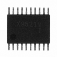
X9521V20I Intersil, X9521V20I Datasheet - Page 9

X9521V20I
Manufacturer Part Number
X9521V20I
Description
IC LASR CTRLR 2CHAN 5.5V 20TSSOP
Manufacturer
Intersil
Type
Laser Diode Controller (Fiber Optic)r
Datasheet
1.X9521V20I.pdf
(24 pages)
Specifications of X9521V20I
Number Of Channels
2
Voltage - Supply
2.7 V ~ 5.5 V
Current - Supply
1.5mA
Operating Temperature
-40°C ~ 85°C
Package / Case
20-TSSOP
Mounting Type
Surface Mount
Lead Free Status / RoHS Status
Contains lead / RoHS non-compliant
Other names
X9521V20I-A
X9521V20I-A
X9521V20I-A
2kbit EEPROM ARRAY
Operations on the 2kbit EEPROM Array, consist of either
1, 2 or 3 byte command sequences. All operations on the
EEPROM must begin with the Device Type Identifier of
the Slave Address set to 1010000. A Read or Write to
the EEPROM is selected by setting the LSB of the Slave
Address to the appropriate value R/W (Read = “1”, Write
= ”0”).
In some cases when performing a Read or Write to the
EEPROM, an Address Byte may also need to be speci-
fied. This Address Byte can contain the values 00h to
FFh.
EEPROM Byte Write
In order to perform an EEPROM Byte Write operation to
the EEPROM array, the Write Enable Latch (WEL) bit of
the CONSTAT Register must first be set (See “BL1, BL0:
Block Lock protection bits - (Nonvolatile)” on page 12.)
For a write operation, the X9521 requires the Slave
Address Byte and an Address Byte. This gives the
master access to any one of the words in the array. After
receipt of the Address Byte, the X9521 responds with an
ACKNOWLEDGE, and awaits the next eight bits of data.
After receiving the 8 bits of the Data Byte, it again
responds with an ACKNOWLEDGE. The master then
terminates the transfer by generating a STOP condition,
at which time the X9521 begins the internal write cycle to
the nonvolatile memory (See Figure 12). During this
internal write cycle, the X9521 inputs are disabled, so it
does not respond to any requests from the master. The
SDA output is at high impedance. A write to a region of
EEPROM memory which has been protected with the
Block-Lock feature (See “BL1, BL0: Block Lock
protection bits - (Nonvolatile)” on page 12.), suppresses
the ACKNOWLEDGE bit after the Address Byte.
Signals from
Signals from
the Master
SDA Bus
the Slave
9
Figure 12. EEPROM Byte Write Sequence
S
a
t
r
t
1 0 1 0 0 0 0
Address
Slave
Address
Internal
Device
WRITE Operation
0
X9521
A
C
K
Address
Byte
EEPROM Page Write
In order to perform an EEPROM Page Write operation to
the EEPROM array, the Write Enable Latch (WEL) bit of
the CONSTAT Register must first be set (See “BL1, BL0:
Block Lock protection bits - (Nonvolatile)” on page 12.)
The X9521 is capable of a page write operation. It is initi-
ated in the same manner as the byte write operation; but
instead of terminating the write cycle after the first data
byte is transferred, the master can transmit an unlimited
number of 8-bit bytes. After the receipt of each byte, the
X9521 responds with an ACKNOWLEDGE, and the
address is internally incremented by one. The page
address remains constant. When the counter reaches
the end of the page, it “rolls over” and goes back to ‘0’ on
the same page.
For example, if the master writes 12 bytes to the page
starting at location 11 (decimal), the first 5 bytes are writ-
ten to locations 11 through 15, while the last 7 bytes are
written to locations 0 through 6. Afterwards, the address
counter would point to location 7. If the master supplies
more than 16 bytes of data, then new data overwrites the
previous data, one byte at a time (See Figure 13).
The master terminates the Data Byte loading by issuing
a STOP condition, which causes the X9521 to begin the
nonvolatile write cycle. As with the byte write operation,
all inputs are disabled until completion of the internal
write cycle. See Figure 10 for the address, ACKNOWL-
EDGE, and data transfer sequence.
Stops and EEPROM Write Modes
Stop conditions that terminate write operations must be
sent by the master after sending at least 1 full data byte
and receiving the subsequent ACKNOWLEDGE signal.
If the master issues a STOP within a Data Byte, or before
the X9521 issues a corresponding ACKNOWLEDGE,
the X9521 cancels the write operation. Therefore, the
contents of the EEPROM array does not change.
C
A
K
Byte
Data
A
C
K
S
o
p
t
September 21, 2010
FN8207.2


