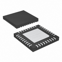
MAX5954LETX+T Maxim Integrated Products, MAX5954LETX+T Datasheet - Page 2

MAX5954LETX+T
Manufacturer Part Number
MAX5954LETX+T
Description
IC PCI EXP/HOT-PLUG CTRLR 36TQFN
Manufacturer
Maxim Integrated Products
Type
Hot-Swap Controllerr
Datasheet
1.MAX5954AETX.pdf
(22 pages)
Specifications of MAX5954LETX+T
Applications
General Purpose, PCI Express
Internal Switch(s)
No
Voltage - Supply
3.3V, 12V
Operating Temperature
-40°C ~ 85°C
Mounting Type
Surface Mount
Package / Case
36-WFQFN Exposed Pad
Mounting Style
SMD/SMT
Lead Free Status / RoHS Status
Lead free / RoHS Compliant
ABSOLUTE MAXIMUM RATINGS
(All voltages referenced to GND, unless otherwise noted.)
12VIN......................................................................-0.3V to +14V
12G............................................................-0.3V to (V
12S, 12S-, 3.3G ......................................-0.3V to (V
3.3VAUXIN, ON,
PWRGD ....................................................................-0.3V to +6V
PGND ....................................................................-0.3V to +0.3V
All Other Pins to GND......................-0.3V to (V
ELECTRICAL CHARACTERISTICS
(V
OUTPUT = 12G = 3.3G = OPEN, INPUT = PRES-DET = PGND = GND, T
are at T
Single PCI Express, Hot-Plug
Controller
Stresses beyond those listed under “Absolute Maximum Ratings” may cause permanent damage to the device. These are stress ratings only, and functional
operation of the device at these or any other conditions beyond those indicated in the operational sections of the specifications is not implied. Exposure to
absolute maximum rating conditions for extended periods may affect device reliability.
2
12V SUPPLY
12V Supply Voltage Range
12VIN Undervoltage Lockout
12VIN Supply Current
12VIN CONTROL
12VIN Current-Limit
Threshold (V
12G Gate Charge Current
12G Gate Discharge Current
12G Gate High Voltage
12G Threshold Voltage For
PWRGD Assertion
12S- Input Bias Current
12S+ Input Bias Current
3.3V SUPPLY
3.3V Supply Voltage Range
Undervoltage Lockout
(Note 3)
(V
12VIN
12G
_______________________________________________________________________________________
A
- V
= V
PARAMETER
= +25°C.) (Note 1)
12VIN
12S-
12S+
)
= V
FAULT ..........................................-0.3V to +6V
- V
12S+
12S-
= 12V, V
)
3.3S+
SYMBOL
I
V
V
I
12G_CHG
V
12G_DIS
V
V
V
12UVLO
I
PGTH12
12VIN
12ILIM
12VIN
12GH
3.3S+
= V
3.3S-
3.3VAUXIN
V
Hysteresis
V
V
Normal turn-off, ON = GND, V
O utp ut shor t- ci r cui t cond i ti on, str ong g ate p ul l d ow n
to r eg ul ati on, V
I
Referred to V
3.3S+ rising
Hysteresis
= V
12G
12VIN
12G
12VIN
12VIN
3.3VAUXIN
12VIN
= 1µA
= GND
rising
= 13.2V
+ 0.3V)
+ 0.3V)
+ 6V)
12VIN
= V
1 2V IN
ON
CONDITIONS
, I
- V
12G_
= V
Continuous Power Dissipation (T
Operating Temperature Range ...........................-40°C to +85°C
Junction Temperature ......................................................+150°C
Storage Temperature Range .............................-65°C to +150°C
Lead Temperature (soldering, 10s) .................................+300°C
1 2S _
36-Pin Thin QFN (derate 26.3mW/°C above +70°C).....2.105W
AUXON
= 1µA (Note 2)
A
≥ 1V , V
= -40°C to +85°C, unless otherwise noted. Typical values
12G
= V
= 2V
1 2G_
FON
= 5V
= 3.3V, PWRGD = FAULT = PORADJ = TIM =
10.8
2.52
MIN
9.5
4.8
3.0
3.0
49
50
50
A
4
= +70°C)
TYP
2.65
150
120
3.3
0.1
0.5
5.3
12
10
54
20
30
5
4
MAX
13.2
10.5
2.78
250
180
5.8
4.8
3.6
59
60
1
6
1
UNITS
mA
mV
mA
mV
µA
µA
µA
µA
V
V
V
V
V
V


