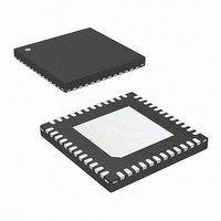
ISL6112IRZA Intersil, ISL6112IRZA Datasheet - Page 4

ISL6112IRZA
Manufacturer Part Number
ISL6112IRZA
Description
IC PWR CNTRLR DUAL SLT 48-QFN
Manufacturer
Intersil
Type
Hot-Swap Controllerr
Datasheet
1.ISL6112IRZA.pdf
(31 pages)
Specifications of ISL6112IRZA
Applications
General Purpose, PCI Express
Internal Switch(s)
No
Voltage - Supply
3.3V, 12V
Operating Temperature
-40°C ~ 85°C
Mounting Type
Surface Mount
Package / Case
48-VFQFN Exposed Pad
Lead Free Status / RoHS Status
Lead free / RoHS Compliant
Pin Descriptions (Pin Numbers and Names are Related)
PIN NUMBER
12, 25
16, 21
10, 27
13, 24
14, 23
15, 22
44, 43
45, 42
11, 26
5, 32
8, 29
3, 34
2, 35
6, 31
AUXENA, AUXENB Level sensitive auxiliary enable Inputs. Used to enable or disable the VAUX outputs. Taking AUXEN low
3VOUTA, 3VOUTB 3.3VOUT. Connected to 3.3V FET source. These are used to monitor the 3.3V output voltages for Power
VSTBYA, VSTBYB 3.3V Standby Input Voltage: Required to support PCI Express VAUX output. Additionally, the SMBus logic
12VINA, 12VINB
VAUXA, VAUXB
3VINA, 3VINB
12VSENSEA,
12VSENSEB
3VSENSEA,
3VSENSEB
12VGATEA
12VGATEB
CFILTERA,
PIN NAME
ONA, ONB
12VOUTA,
CFILTERB
12VOUTB
3VGATEA
3VGATEB
PWRGDA
PWRGDB
4
Provides 12VMAIN power supply and the high side of the sense resistor inputs. This must be a Kelvin
connection between IC and sense resistor. An undervoltage lockout circuit (UVLO) prevents the switches
from turning on while this input is less than its lockout threshold.
Provides 3.3VMAIN power supply and the high side of the sense resistor inputs. This must be a Kelvin
connection between IC and sense resistor. An undervoltage lockout circuit (UVLO) prevents the switches
from turning on while this input is less than its lockout threshold.
Good status.
12VOUT. Connected to 12V FET drain. These are used to monitor the 3.3V output voltages for Power
Good status.
12VMAIN low side of sense resistor connection. When either current limit threshold of the load current
across the sense resistor = 50mV is reached, the related 12VGATE pin is modulated to maintain a
constant voltage across the sense resistor and thus a constant current into the load. If the 50mV threshold
is exceeded for tFLT, the isolation protection is tripped and the GATE pin for the affected supply’s external
MOSFET is immediately pulled high. This must be a Kelvin connection between IC and sense resistor.
3.3VMAIN low side of sense resistor connection. When either current limit threshold of the load current
across the sense resistor = 50mV is reached, the related 3V GATE pin is modulated to maintain a constant
voltage across the sense resistor and thus a constant current into the load. If the 50mV threshold is
exceeded for tFLT, the isolation protection is tripped and the GATE pin for the affected supply’s external
MOSFET is immediately pulled low. This must be a Kelvin connection between IC and sense resistor.
12V Gate Drive Outputs: Each pin connects to the gate of an external P-Channel MOSFET. During
power-up, the CGATE and the CGS of the MOSFETs are connected to a 25µA current sink. This controls
the value of dv/dt seen at the source of the MOSFETs. During current limit events, the voltage at this pin
is adjusted to maintain constant current through the switch for a period of tFLT. Whenever an overcurrent,
thermal shutdown, or input undervoltage fault condition occurs, the GATE pin for the affected slot is
immediately brought high. These pins are charged by an internal current source during power-down.
3V Gate Drive Outputs: Each pin connects to the gate of an external N-Channel MOSFET. During power-
up, the CGATE and the CGS of the MOSFETs are connected to a 25µA current source. This controls the
value of dv/dt seen at the source of the MOSFETs, and hence the current flowing into the load capacitance.
During current limit events, the voltage at this pin is adjusted to maintain constant current through the
switch for a period of tFLT. Whenever an overcurrent, thermal shutdown, or input undervoltage fault
condition occurs, the GATE pin for the affected slot is immediately brought low. During power-down, these
pins are discharged by an internal current source.
and internal registers run off of VSTBY to ensure that the chip is accessible during standby modes. A
UVLO circuit prevents turn-on of this supply until VSTBY rises above its UVLO threshold. Both pins must
be externally connected together at the ISL6112 controller.
3.3VAUX Outputs to PCI Express Card Slots: These outputs connect the 3.3AUX pin of the PCI Express
connectors to VSTBY via internal 400mΩ MOSFETs. These outputs are 1A current limited and protected
against short-circuit faults.
Enable Inputs: Rising-edge triggered. Used to enable or disable the MAINA and MAINB (+3.3V and +12V)
outputs. Taking ON low after a fault resets the +12V and/or +3.3V fault latches for the affected slot. Tie
these pins to GND if using SMI power control. Also, see pin description for FAULTA and FAULTB.
after a fault resets the respective slot’s Aux Output Fault Latch. Tie these pins to GND if using SMI power
control. Also, see pin description for FAULTA and FAULTB.
Overcurrent Timers: Capacitors connected between these pins and GND set the duration of CR
CR
invoked.
Power-is-Good Outputs: Open-drain, active-low. Asserted when a slot has been commanded to turn on
and has successfully begun delivering power to its respective +12V, +3.3V, and VAUX outputs. Each pin
requires an external pull-up resistor to V
TIM
is the amount of time for which a slot remains in current limit before its isolation protection is
ISL6112
STBY
PIN FUNCTION
.
September 28, 2007
TIM
FN6456.0
.


