ISL6112IRZA Intersil, ISL6112IRZA Datasheet
ISL6112IRZA
Specifications of ISL6112IRZA


Related parts for ISL6112IRZA


ISL6112IRZA Summary of contents
Page 1
... Additionally the IC has a minimum of I/O for implementations where Hot-Plug Hardware Interface (HPI) is implemented. Ordering Information PART NUMBER (Note) PART MARKING ISL6112IRZA ISL6112 IRZ ISL6112IRZA-T* ISL6112 IRZ ISL6112INZA ISL6112 INZ ISL6112INZA-T* ISL6112 INZ ISL6112EVAL1Z Evaluation Platform *Please refer to TB347 for details on reel specifications. ...
Page 2
Functional Block Diagram (1 Channel) 12VSENSE 50mV 12VIN 3VSENSE 50mV 3VIN ON/OFF 100mV* ON/OFF 100mV* VSTBY I REF CFILTER 1.25V FORCE_ON GPI BOTH A AND B SLOTS SHARE THE SCL, SDA, A0, A1, A2, INT PINS. 2 ISL6112 ON AUXEN ...
Page 3
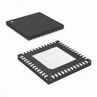
Pinouts FAULTA CFILTERA 12VGATEA GPI_A0 12VINA PWRGDA NC 12VSENSEA FORCE_ONA 12VOUTA VSTBYA 3VINA CFILTERA 12VGATEA PWRGDA 12VSENSEA FORCE_ONA 12VOUTA VSTBYA 3 ISL6112 ISL6112 (48 LD 7X7 TQFP) TOP VIEW ...
Page 4
Pin Descriptions (Pin Numbers and Names are Related) PIN NUMBER PIN NAME 5, 32 12VINA, 12VINB Provides 12VMAIN power supply and the high side of the sense resistor inputs. This must be a Kelvin connection between IC and sense resistor. ...
Page 5
Pin Descriptions (Pin Numbers and Names are Related) PIN NUMBER PIN NAME 1, 36 FAULTA, FAULTB Fault Outputs: Open-drain, active-low. Asserted whenever the isolation protection trips due to a fault condition (overcurrent, input undervoltage, over-temperature). Each pin requires an external ...
Page 6
... Ld 7x7 QFN Package (Notes Maximum Junction Temperature . . . . . . . . . . . . . . . . . . . . . . +150°C Maximum Storage Temperature Range . . . . . . . . . -65°C to +150°C Pb-free reflow profile . . . . . . . . . . . . . . . . . . . . . . . . . .see link below http://www.intersil.com/pbfree/Pb-FreeReflow.asp Operating Conditions 12VMAIN Supply Voltage Range +12V ± -10% 3.3VMAIN Supply Voltage Range . . . . . . . . . . . . . . . . +3.3V ± -10% AUXI Supply Voltage Range . . . . . . . . . . . . . . . . . . . . +3.3V ± -10% ...
Page 7
Electrical Specifications 12VIN = 12V, 3VIN = 3.3V, VSTBY = 3.3V, T PARAMETER CFILTER OVERCURRENT DELAY TIME PINS 2 AND 35 FLOATING CFILTER Threshold Voltage CFILTER Charging Current Nominal Current Limit Duration = C x 550k CFILTER Current Limit Threshold ...
Page 8
Electrical Specifications 12VIN = 12V, 3VIN = 3.3V, VSTBY = 3.3V, T PARAMETER SMBUS TIMING SCL (clock) period Data In setup time to SCL HIGH Data Out stable after SCL LOW Data LOW setup time to SCL LOW Data HIGH ...
Page 9
Typical Application Diagram +12V SYSTEM POWER +3.3V SUPPLY VSTBY V STBY C1 100k 100k 100k 100k FORCE_ONA FORCE_ONB GPI_A0 GPI_B0 V STBY AUXENA AUXENB ONA ONB V STBY HOT-PLUG CONTROLLER PWRGDA PWRGDB FAULTA FAULTB SMBUS BASE ADDRESS VSTBY 10k x ...
Page 10
Functional Description The ISL6112 protects the power supplies in PCI-Express systems that utilize hot-pluggable add-in cards. This IC together with two each of N-Channel and P-Channel MOSFETs, four current sense resistors and a few external passive components, provide a compliant ...
Page 11
V STBY 100k 100k INT DISABLING SMI WHEN HPI CONTROL IS USED 100k 9 V STBY 100k DISABLING HPI WHEN SMI CONTROL IS USED FIGURE 1. I/O CONFIGURATION FOR DISABLING HPI/SMI CONTROL ISL6112 Bias, ...
Page 12
I = 50mV/R and C LIM SENSE LOAD capacitance consequence, the CR duration, t must be programmed to exceed the time it will take to fully charge the output load to the input rail voltage level. MAIN ...
Page 13
C RESPONDING TO UNSHOWN MAIN SUPPLY FILTER FIGURE 6. 3VMAIN START-UP R LOAD FIGURE 7. 12VMAIN START-UP R LOAD C = 470µF LOAD Current Regulation (CR) Function The ISL6112 provides a current regulation and limiting function that protects the input ...
Page 14
GATE 3I OUT FIGURE 11. 3VMAIN WOC SHUT-DOWN The VAUX outputs have a different isolation protection function. The VAUX isolation circuit does not incorporate a fast-trip detector, instead they regulate the output current into a fault to avoid exceeding ...
Page 15
For the ISL6112, there is a minimum t FILTER since the ISL6112 has its CR feature invoked as it turns-on the FETs into the load. There is a maximum bulk capacitance specified for each power level supported that needs to ...
Page 16
Timing Diagrams SCL SDA DATA IN SDA DATA OUT UVLO VSTBY AUXEN 0 tPOR VAUX_OUT 0 ILIM(AUX) I STEADY-STATE I AUX_OUT 12VOUT 0 3VOUT 0 PWRGD_ 0 ILIM(3V) ISTEADY-STATE I3VOUT 0 FAULT_ 0 INT* 0 ISL6112 DEVICE ...
Page 17
Timing Diagrams (Continued) ISL6112 DEVICE ADDRESS DATA R/W = WRITE START CLK DATA Hot-Plug Interface (HPI) Once the input supplies are above their respective UVLO thresholds, the Hot-Plug Interface can be utilized ...
Page 18
For those SMI control applications where the FORCE_ON inputs are needed for diagnostic purposes, the FORCE_ON inputs must be enabled; that is, CNTRL Register Bit D[2] should read Logical “0.” Once FORCE_ON inputs are asserted, all output voltages are present ...
Page 19
ISL6112 Register Set and Programmer’s Model TARGET REGISTER LABEL CNTRLA Control Register Slot A CNTRLB Control Register Slot B STATA Slot A Status STATB Slot B Status CS Common Status Register Reserved Reserved/Do Not Use Detailed Register Descriptions Control Register, ...
Page 20
Status Register Slot A (STATUSA) 8-Bits, Read-Only D[7] D[6] read-only read-only FAULTA MAINA BIT(s) FAULTA FAULT Status - Slot A MAINA MAIN Enable Status - Slot A VAUXA VAUX Enable Status - Slot A VAUXAF Overcurrent Fault: VAUXA supply D[3] ...
Page 21
Control Register, Slot B (CNTRLB) 8-Bits, Read/Write D[7] D[6] read-only read-only AUXBPG MAINBPG BIT(s) AUXBPG AUX output power-good status, Slot B MAINBPG MAIN output power-good status, Slot B D[5] Reserved D[4] Reserved D[3] Reserved FORCE_B Allows or inhibits the operation ...
Page 22
Status Register Slot B (STATB) 8-Bits, Read-Only D[7] D[6] read-only read-only FAULTB MAINB BIT(s) FAULTB FAULT Pin Status - Slot B MAINB MAIN Enable Status - Slot B VAUXB VAUX Enable Status - Slot B VAUXBF Overcurrent Fault: VAUXB supply ...
Page 23
Common Status Register (CS) 8-Bits, Read/Write D[7] D[6] read-write read-write read-only Reserved Reserved GPI_B0 BIT(s) D[7] Reserved D[6] Reserved GPI_B0 General Purpose Input 0, Slot B GPI_A0 General Purpose Input 0, Slot A INTMSK Interrupt Mask UV_INT undervoltage Interrupt OT_INT ...
Page 24
... The specific evaluation board as ordered and received will reflect the part number in the area below the Intersil logo either by label or silk screened lettering. For those pins not common across the ISL6112 and ISL6113, ISL6114, there is a matrix detailing the differences in the bottom left corner ...
Page 25
Typical Performance Curves 6.0 5.8 5.6 5.4 SMI ICCSTBY 5.2 5.0 4.8 HPI ICCSTBY 4.6 4.4 4.2 4.0 -60 -40 - TEMPERATURE (°C) FIGURE 20. ICCSTBY CURRENT vs TEMPERATURE -60 ...
Page 26
Typical Performance Curves 9.30 9.25 9.20 9.15 9.10 9.05 -60 -40 - TEMPERATURE (°C) FIGURE 26. 12MAIN RISING UVLO THRESHOLD VOLTAGE vs TEMPERATURE 10.54 10.52 10.50 10.48 10.46 10.44 10.42 10.40 10.38 -60 -40 - ...
Page 27
Typical Performance Curves 3.0 2.9 2.8 2.7 2.6 2.5 2.4 2.3 2.2 2.1 2.0 -60 -40 - TEMPERATURE (°C) FIGURE 32. FILTER CHARGE CURRENT vs TEMPERATURE 27 ISL6112 (Continued) 1.30 1.28 1.26 1.24 1.22 1. ...
Page 28
CAUTION HOT TABLE 11. ISL6112EVAL1Z BOARD COMPONENTS LISTING COMPONENT DESIGNATOR U1 Q1, Q4 Q2, Q3 R1, R3, R6, R8 R9, R10, R17, R20 R11, R12, R13, 14, R15, R16, R18, 19, R21 R2, R4, R5, R7 C1, C7, C8, C13 ...
Page 29
...
Page 30
Package Outline Drawing L48.7x7 48 LEAD QUAD FLAT NO-LEAD PLASTIC PACKAGE Rev 4, 10/06 7.00 6 PIN 1 INDEX AREA (4X) 0.15 TOP VIEW ( TYP ) ( TYPICAL RECOMMENDED LAND PATTERN 30 ...
Page 31
... Accordingly, the reader is cautioned to verify that data sheets are current before placing orders. Information furnished by Intersil is believed to be accurate and reliable. However, no responsibility is assumed by Intersil or its subsidiaries for its use; nor for any infringements of patents or other rights of third parties which may result from its use ...