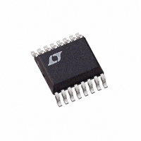
LTC4221CGN Linear Technology, LTC4221CGN Datasheet - Page 23

LTC4221CGN
Manufacturer Part Number
LTC4221CGN
Description
IC CTRLR HOTSWAP DUAL 16SSOP
Manufacturer
Linear Technology
Type
Hot-Swap Controllerr
Datasheet
1.LTC4221CGNPBF.pdf
(28 pages)
Specifications of LTC4221CGN
Applications
General Purpose
Internal Switch(s)
No
Voltage - Supply
1 V ~ 13.5 V
Operating Temperature
0°C ~ 70°C
Mounting Type
Surface Mount
Package / Case
16-SSOP (0.150", 3.90mm Width)
Lead Free Status / RoHS Status
Contains lead / RoHS non-compliant
Available stocks
Company
Part Number
Manufacturer
Quantity
Price
Company:
Part Number:
LTC4221CGN
Manufacturer:
LT
Quantity:
10 000
Part Number:
LTC4221CGN#PBF
Manufacturer:
LTNEAR
Quantity:
20 000
APPLICATIO S I FOR ATIO
the input supply line, exhibiting a peak overshoot to 2.5
times the steady-state value. This peak is followed by a
damped sinusoidal response whose duration and period
are dependent on the resonant circuit parameters. This
can cause detrimental damage to board components
unless measures are taken.
The energy stored in the lead/trace inductance is easily
controlled with snubbers and/or transient voltage sup-
pressors. Even when ferrite beads are used for electro-
magnetic interference (EMI) control, the low saturating
current of ferrite will not pose a major problem if the
transient voltage suppressors with adequate ratings are
used. The transient associated with a GATE turn off can be
controlled with a snubber and/or transient voltage sup-
pressor. Snubbers such as RC networks are effective
especially at low voltage supplies. The choice of RC is
usually determined experimentally. The value of the snub-
ber capacitor is usually chosen between 10 to 100 times
the MOSFET C
typically between 3Ω to 100Ω. When the supply exceeds
7V or EMI beads exist in the wire harness, a transient
voltage suppressor and snubber are recommended to clip
off large spikes and reduce the ringing. For supply volt-
ages of 6V or below, a snubber network should be suffi-
cient to protect against transient voltages. These protection
networks should be mounted very close to each of
LTC4221’s two supply voltages using short lead lengths to
minimize lead inductance. This is shown schematically in
the Typical Application on the front page of this data sheet.
In many cases, a simple short-circuit test can be per-
formed to determine the need of the transient voltage
suppressor. Additional overvoltage protection is provided
by the FB n pins.
OSS
. The value of the snubber resistor is
U
U
W
U
PCB Layout Considerations
A recommended layout for the SENSE resistors, the
power MOSFETs, V
GATE drive components around the LTC4221 is shown in
Figure 16. For proper operation of the LTC4221’s elec-
tronic circuit breaker, a 4-wire Kelvin connection to each
SENSE resistor is used. Also, PCB layout for the external
N-channel MOSFETs emphasizes optimal thermal man-
agement of MOSFET power dissipation to keep θ
as possible. The V
positioned close to the supply pins to reduce lead induc-
tance and thus overshoot voltage.
In Hot Swap applications where load currents can reach
10A or more, PCB track width must be appropriately sized
to keep track resistance and temperature rise to a mini-
mum. Consult Appendix A of LTC Application Note 69 for
details on sizing and calculating trace resistances as a
function of copper thickness.
In the majority of applications, it will be necessary to use
plated-through vias to make circuit connections from
component layers to power and ground layers internal to
the PC board. For 1oz copper foil plating, a good starting
point is 1A of DC current per via, making sure the via is
properly dimensioned so that solder completely fills any
void. For other plating thicknesses, check with your PCB
fabrication facility.
CC
CC
transient protection devices are
transient protection devices and
LTC4221
JA
23
as low
4221fa


