LTC4252A-1IMS Linear Technology, LTC4252A-1IMS Datasheet - Page 22

LTC4252A-1IMS
Manufacturer Part Number
LTC4252A-1IMS
Description
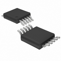
IC CTRLR HOTSWAP NEG VOLT 10MSOP
Manufacturer
Linear Technology
Type
Hot-Swap Controllerr
Specifications of LTC4252A-1IMS
Applications
General Purpose
Internal Switch(s)
No
Operating Temperature
-40°C ~ 85°C
Mounting Type
Surface Mount
Package / Case
10-TFSOP, 10-MSOP (0.118", 3.00mm Width)
Family Name
LTC4252A-1
Package Type
MSOP
Operating Temperature (min)
-40C
Operating Temperature (max)
85C
Operating Temperature Classification
Industrial
Product Depth (mm)
3mm
Product Height (mm)
0.86mm
Product Length (mm)
3mm
Mounting
Surface Mount
Pin Count
10
Lead Free Status / RoHS Status
Contains lead / RoHS non-compliant
Lead Free Status / RoHS Status
Contains lead / RoHS non-compliant
Available stocks
Company
Part Number
Manufacturer
Quantity
Price
Company:
Part Number:
LTC4252A-1IMS
Manufacturer:
LT
Quantity:
10 000
Part Number:
LTC4252A-1IMS#PBF
Manufacturer:
LINEAR/凌特
Quantity:
20 000
Company:
Part Number:
LTC4252A-1IMS#TRPBF
Manufacturer:
LINEAR
Quantity:
12 958
Part Number:
LTC4252A-1IMS#TRPBF
Manufacturer:
LINEAR/凌特
Quantity:
20 000
APPLICATIO S I FOR ATIO
LTC4252-1/LTC4252-2
LTC4252A-1/LTC4252A-2
At time point 8, the load current falls and the SENSE
voltage drops below V
shuts off and the GATE pin ramps further. At time point 9,
the SENSE voltage drops below V
ends, followed by a 5.8µA discharge cycle (cool off). The
duration between time points 7 and 9 must be shorter than
one circuit breaker delay to avoid a fault time out during
GATE ramp-up. When GATE ramps past the V
old at time point 10, PWRGD pulls low. At time point 11,
GATE reaches its maximum voltage as determined by V
Live Insertion with Short Pin Control of UV/OV
In the example shown in Figure 10, power is delivered
through long connector pins whereas the UV/OV divider
22
(–48RTN) – (–48V)
GND – V
PWRGD
SENSE
TIMER
DRAIN
UV/OV
EE
GATE
V
OUT
V
OR
SS
IN
U
1
ACL
V
2
IN
(t). The analog current limit loop
U
V
V
CLEARS V
Figure 9. System Power-Up Timing (All Waveforms are Referenced to V
GATEL
LKO
CB
LKO
, the fault TIMER cycle
, CHECK UV > V
W
5.8µA
INITIAL TIMING
GATEH
UVHI
U
, OV < V
20 • (V
20 • (V
thresh-
V
TMRH
OVLO
ACL
CB
20 • V
IN
V
+ V
+ V
, GATE < V
.
TMRL
OS
OS
OS
)
)
58µA
3 4 56
makes contact through a short pin. This ensures the power
connections are firmly established before the LTC4252 is
activated. At time point 1, the power pins make contact and
V
makes contact and its voltage exceeds V
the internal logic checks for OV < V
SENSE < V
conditions are met, an initial timing cycle starts and the
TIMER capacitor is charged by a 5.8µA current source
pull-up. At time point 3, TIMER reaches the V
old and the initial timing cycle terminates. The TIMER
capacitor is quickly discharged. At time point 4, the V
threshold is reached and the conditions of GATE < V
SENSE < V
TIMER CLEARS V
IN
230µA + 8 • I
GATEL
ramps through V
START-UP
, SENSE < V
GATE
7
58µA
8
DRN
9
CB
CB
10 11
TMRL
CB
, SS < 20 • V
and SS < 20 • V
, SS < 20 • V
, CHECK GATE < V
V
V
V
V
V
IN
ACL
CB
DRNCL
DRNL
– V
GATEH
LKO
5.8µA
OS
. At time point 2, the UV/OV divider
AND TIMER < V
GATEL
OS
EE
OS
, SENSE < V
)
and TIMER < V
must be satisfied before
TMRL
5.8µA
OVHI
CB
4252-1/2 F09
AND SS < 20 • V
, GATE < V
UVHI
TMRH
. In addition,
TMRL
OS
thresh-
GATEL
GATEL
. If all
425212fb
TMRL
,
,


