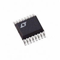
LT4256-3IGN Linear Technology, LT4256-3IGN Datasheet - Page 10

LT4256-3IGN
Manufacturer Part Number
LT4256-3IGN
Description
IC CTRLR HOTSWP HV DETECT 16SSOP
Manufacturer
Linear Technology
Type
Hot-Swap Controllerr
Datasheet
1.LT4256-3IGNPBF.pdf
(20 pages)
Specifications of LT4256-3IGN
Applications
General Purpose
Internal Switch(s)
No
Voltage - Supply
10.8 V ~ 80 V
Operating Temperature
-40°C ~ 85°C
Mounting Type
Surface Mount
Package / Case
16-SSOP (0.150", 3.90mm Width)
Lead Free Status / RoHS Status
Contains lead / RoHS non-compliant
Available stocks
Company
Part Number
Manufacturer
Quantity
Price
Company:
Part Number:
LT4256-3IGN
Manufacturer:
LT
Quantity:
10 000
Part Number:
LT4256-3IGN
Manufacturer:
LINEAR/凌特
Quantity:
20 000
Company:
Part Number:
LT4256-3IGN#PBF
Manufacturer:
LT
Quantity:
1
Part Number:
LT4256-3IGN#PBF
Manufacturer:
LINEAR/凌特
Quantity:
20 000
Part Number:
LT4256-3IGN#TRPBF
Manufacturer:
LINEAR/凌特
Quantity:
20 000
APPLICATIO S I FOR ATIO
LT4256-3
Hot Circuit Insertion
When circuit boards are inserted into a live backplane, the
supply bypass capacitors on the boards draw high peak
currents from the backplane power bus as they charge.
The transient currents can permanently damage the con-
nector pins and glitch the system supply, causing other
boards in the system to reset.
The LT4256-3 is designed to turn on a board’s supply
voltage in a controlled manner, allowing the board to be
safely inserted or removed from a live backplane. The
device also provides undervoltage and overvoltage as well
as overcurrent protection while a power good output
signal indicates when the output supply voltage is ready
with a high output.
Power-Up Sequence
An external N-channel MOSFET pass transistor (Q1) is
placed in the power path to control the power up of the
supply voltage (Figure 5). Resistor R5 provides current
detection and capacitor C1 controls the GATE slew rate.
Resistor R7 compensates the current control loop while
R6 prevents high frequency oscillations in Q1.
10
U
GND
48V
V
IN
0.01µF
U
(SHORT PIN)
C3
W
R1
64.9k
R2
4.02k
R3
4.02k
C2
33nF
D2
SMAT70A
Figure 5. 1.6A, 48V Latchoff Application
1
2
4
9
UV
OV
OPEN
TIMER
V
U
CC
LT4256-3
16
0.025Ω
GND
R5
8
SENSE
PWRGD
RETRY
GATE
V
15
OUT
FB
13
12
10
7
5
IRF530
When the power pins first make contact, transistor Q1 is
held off. If the voltage on V
programmed undervoltage and overvoltage thresholds,
V
4.65V (typ), transistor Q1 will be turned on (Figure 6). The
voltage on GATE rises with a slope equal to 32µA/C1 and
the supply inrush current is set at:
where C
500mA/DIV
Q1
CC
PWRGD
50V/DIV
50V/DIV
50V/DIV
R6
10Ω
R7
100Ω
I
INRUSH
GATE
C1
10nF
V
is above 9.8V and the voltage on TIMER is less than
I
OUT
OUT
UV = 36V
OV = 73V
PWRGD = 40V
D1
CMPZ5241BS
11V
L
C
is the total load capacitance.
L
= C
= 125µF
L
Figure 6. Start-Up Waveforms
• 32µA/C1
R8
36.5k
R9
4.02k
4256 F05
5ms/DIV
R4
51k
+
CC
PWRGD
C
is between the externally
L
V
48V
1.6A
OUT
4256 F06
42563fa
(1)


