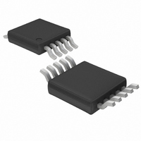
LTC4214-2CMS Linear Technology, LTC4214-2CMS Datasheet - Page 17

LTC4214-2CMS
Manufacturer Part Number
LTC4214-2CMS
Description
IC CTRLR HOTSWAP NEGVOLT 10MSOP
Manufacturer
Linear Technology
Type
Hot-Swap Controllerr
Datasheet
1.LTC4214-1CMS.pdf
(32 pages)
Specifications of LTC4214-2CMS
Applications
General Purpose
Internal Switch(s)
No
Voltage - Supply
6 V ~ 16 V
Operating Temperature
0°C ~ 70°C
Mounting Type
Surface Mount
Package / Case
10-TFSOP, 10-MSOP (0.118", 3.00mm Width)
Linear Misc Type
Negative Low Voltage
Family Name
LTC4214-2
Package Type
MSOP
Operating Supply Voltage (min)
-6V
Operating Supply Voltage (max)
-16V
Operating Temperature (min)
0C
Operating Temperature (max)
70C
Operating Temperature Classification
Commercial
Product Depth (mm)
3mm
Product Height (mm)
0.86mm
Product Length (mm)
3mm
Mounting
Surface Mount
Pin Count
10
Lead Free Status / RoHS Status
Contains lead / RoHS non-compliant
Lead Free Status / RoHS Status
Contains lead / RoHS non-compliant
Available stocks
Company
Part Number
Manufacturer
Quantity
Price
Company:
Part Number:
LTC4214-2CMS
Manufacturer:
LT
Quantity:
10 000
APPLICATIO S I FOR ATIO
TIMER commences charging C
current limit loop maintains the fault current at 70mV/R
which in this case is 3.5A (Trace 2). Note that the back-
plane voltage (Trace 1) sags under load. Timer pull-up is
accelerated by V
PWRGD pulls high, the load current drops to zero and the
backplane rings in the positive direction. The transient
associated with the GATE turn off can be controlled with a
snubber to reduce ringing and transient voltage suppres-
sor to clip off large spikes. The choice of RC for the
snubber is usually done experimentally. The value of the
snubber capacitor is usually chosen between 10 to 100
times the MOSFET C
is typically between 3 to 100 . In many cases, a simple
short-circuit test can be performed to determine the
component values needed.
A low impedance short on one card may influence the
behavior of others sharing the same backplane. The initial
glitch and backplane sag as seen in Figure 5 Trace 1, can
rob charge from output capacitors on adjacent cards.
When the faulty card shuts down, current flows in to
refresh the capacitors. If LTC4214s are used by the other
cards, they respond by limiting the inrush current to a
value of 70mV/R
will recharge long before C
POWER GOOD, PWRGD
PWRGD latches low if GATE charges up to within 2.8V of
V
is reset in UVLO, in a UV condition or if C
3V. An overvoltage condition has no effect on PWRGD
status. A 50 A current pulls this pin high during reset.
Various ways of using the PWRGD pin for interfacing with
a Power Module load are shown in the Typical Application
as well as Figures 2, 3, 18 and 19.
MOSFET SELECTION
The external MOSFET switch must have adequate safe
operating area (SOA) to handle short-circuit conditions
IN
and DRAIN pulls below V
OUT
S
. If C
U
. When C
OSS
T
. The value of the snubber resistor
is sized correctly, the capacitors
U
T
DRNL
T
times out.
reaches 3V, GATE turns off,
T
(Trace 4) while the analog
during start-up. PWRGD
W
T
charges up to
U
S
,
until TIMER times out. These considerations take prece-
dence over DC current ratings. A MOSFET with adequate
SOA for a given application can always handle the required
current, but the opposite may not be true. Consult the
manufacturer’s MOSFET data sheet for safe operating area
and effective transient thermal impedance curves.
MOSFET selection is a 3-step process by assuming the
absense of a soft-start capacitor. First, R
then the time required to charge the load capacitance is
determined. This timing, along with the maximum short-
circuit current and maximum input voltage defines an
operating point that is checked against the MOSFET’s SOA
curve.
To begin a design, first specify the required load current
and Ioad capacitance, I
current trip point (V
the maximum load current. Note that maximum input
current to a DC/DC converter is expected at V
R
where V
mum circuit breaker threshold.
During the initial charging process, the LTC4214 may
operate the MOSFET in current limit, forcing (V
tween 60mV to 80mV across R
current is given by:
Maximum short-circuit current limit is calculated using
the maximum V
The TIMER capacitor C
slowest expected charging rate; otherwise TIMER might
time out before the load capacitor is fully charged. A value
S
I
I
R
is given by:
INRUSH MIN
SHORTCIRCUIT MAX
S
CB(MIN)
V
I
CB MIN
L MAX
(
(
LTC4214-1/LTC4214-2
(
)
= 44mV represents the guaranteed mini-
)
SENSE
)
(
60
R
CB
mV
S
. This gives
/R
)
T
S
80
L
) should be set to accommodate
must be selected based on the
R
and C
mV
S
S
L
. The minimum inrush
. The circuit breaker
S
is calculated and
SUPPLY(MIN)
ACL
17
) be-
421412f
(10)
(8)
(9)
.


