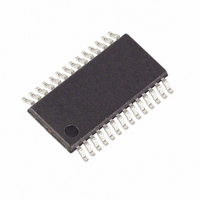
MAX5916AEUI+ Maxim Integrated Products, MAX5916AEUI+ Datasheet - Page 4

MAX5916AEUI+
Manufacturer Part Number
MAX5916AEUI+
Description
IC HOT-SWAP CTRLR DUAL 28-TSSOP
Manufacturer
Maxim Integrated Products
Type
Hot-Swap Controllerr
Datasheet
1.MAX5916EUI.pdf
(25 pages)
Specifications of MAX5916AEUI+
Applications
PCI 2.2 Server
Internal Switch(s)
No
Voltage - Supply
10.8 V ~ 13.2 V
Operating Temperature
-40°C ~ 85°C
Mounting Type
Surface Mount
Package / Case
28-TSSOP
Lead Free Status / RoHS Status
Lead free / RoHS Compliant
Dual PCI 2.2 Hot-Swap Controllers
ELECTRICAL CHARACTERISTICS (continued)
(V
Typical values are at T
Note 1: t
Note 2: The current threshold when the output current starts to fold back. See the Typical Operating Characteristics.
Note 3: t
Note 4: Temperature threshold at which the outputs of the channel with overcurrent shut down.
Note 5: The temperature threshold at which both channels shut down.
4
On-Resistance of Internal Switch
Foldback Current Limit
Current-Foldback Threshold
Output Undervoltage Threshold
Auxiliary Input UVLO Delay Time
3.3VAUXO_ Internal Pulldown
ON AND AUXON COMPARATORS
Threshold Voltage
Hysteresis
Input Bias Current
ON_ and AUXON_ Deglitch
Time
PGOOD_ Output Overcurrent
and Undervoltage Response
Time
Output Overcurrent and
Undervoltage Deglitch Time
PGOOD_ Startup Timeout
Autorestart Delay
PGOOD_ Output Low Voltage
PGOOD_ Output High Leakage
Current
Thermal Shutdown Threshold
Thermal Shutdown Hysteresis
Full Thermal Shutdown
Threshold
Full Thermal Shutdown
Hysteresis
FAULT RESPONSE, PGOOD_ STATUS OUTPUT COMPARATORS
-12VIN
_______________________________________________________________________________________
= -12V, V
DEG, UVLO
DEG
PARAMETER
is negative edge triggered. ON_ or AUXON_ transition from low to high has no delay.
+12VIN
is negative edge triggered. There is no time delay when the inputs rise above the UVLO threshold.
A
= +25°C.)
= +12V, V
R
3.3VAUXIN
V
I
DS(ON), 3.3VAUX
3.3VAUXIN, LIM
3.3VAUXIN, UV
R
t
T
SYMBOL
DEG, UVLO
T
t
3.3VAUXO_
I
HYS, FULL
RESTART
B, COMP
SD, FULL
t
t
t
t
DELAY
I
V
RESP2
START
T
t
RESP
LEAK
V
T
DEG
HYS
HYS
SD
OL
= +3.3V, V
T
T
V
Output current rising (Note 2)
(Note 1)
ON_ = 0V
Figures 5–8 (Note 3)
Figures 5–8
Figures 5–8
Figures 3–7
See Figures 1, 2, 5, 6, 7, and 8
Delay time to restart after OC and/or
UV shutdown
I
V
(Note 4)
(Note 5)
SINK
A
A
3.3VAUXO
PGOOD_
= +25°C, I
= +85°C, I
ON_
= 2mA, ON_ = 0V
= V
= +5.5V
_ = 0V
CONDITIONS
AUXON_
D
D
MAX5915/MAX5916
MAX5915A/MAX5916A
= 0.4A
= 0.4A
= +5V, T
A
= T
MIN
to T
2.76
MIN
1.0
0.5
0.5
MAX
, unless otherwise specified.
t
t
T
t
DELAY
START
TYP
0.24
0.75
2.89
16 x
RESP
64 x
100
125
SD
1.2
1.6
4 x
0.5
25
20
1
4
5
5
+
MAX
2.99
0.4
0.6
1.0
2.1
1.5
0.7
20
1
UNITS
mV
ms
kΩ
ms
ms
ms
ms
µA
µs
µA
°C
°C
°C
°C
ns
Ω
A
A
V
V
V


