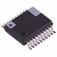
ADE7763ARS Analog Devices Inc, ADE7763ARS Datasheet - Page 45

ADE7763ARS
Manufacturer Part Number
ADE7763ARS
Description
IC ENERGY METER 1PHASE 20SSOP
Manufacturer
Analog Devices Inc
Specifications of ADE7763ARS
Input Impedance
390 KOhm
Measurement Error
0.1%
Voltage - I/o High
2.4V
Voltage - I/o Low
0.8V
Current - Supply
3mA
Voltage - Supply
4.75 V ~ 5.25 V
Operating Temperature
-40°C ~ 85°C
Mounting Type
Surface Mount
Package / Case
20-SSOP (0.200", 5.30mm Width)
Meter Type
Single Phase
For Use With
EVAL-ADE7763ZEB - BOARD EVALUATION FOR ADE7763
Lead Free Status / RoHS Status
Contains lead / RoHS non-compliant
Available stocks
Company
Part Number
Manufacturer
Quantity
Price
Part Number:
ADE7763ARS
Manufacturer:
ADI/亚德诺
Quantity:
20 000
Part Number:
ADE7763ARSZ
Manufacturer:
ADI/亚德诺
Quantity:
20 000
Part Number:
ADE7763ARSZRL
Manufacturer:
ADI/亚德诺
Quantity:
20 000
The serial interface of the ADE7763 is made up of four signals:
SCLK, DIN, DOUT, and CS . The serial clock for a data transfer
is applied at the SCLK logic input. This logic input has a Schmitt-
trigger input structure that allows slow rising and falling clock
edges to be used. All data transfer operations are synchronized
to the serial clock. Data is shifted into the ADE7763 at the DIN
logic input upon the falling edge of SCLK. Data is shifted out of
the ADE7763 at the DOUT logic output upon a rising edge of
SCLK. The CS logic input is the chip-select input. This input is
used when multiple devices share the serial bus. A falling edge
upon CS also resets the serial interface and places the ADE7763
into communication mode. The CS input should be driven low
for the entire data transfer operation. Bringing CS high during a
data transfer operation aborts the transfer and places the serial
bus in a high impedance state. The CS logic input can be tied
low if the ADE7763 is the only device on the serial bus. However,
with CS tied low, all initiated data transfer operations must be
fully completed, i.e., the LSB of each register must be transferred
because there is no other way to bring the ADE7763 into commu-
nication mode without resetting the entire device using RESET .
ADE7763 Serial Write Operation
The serial write sequence takes place as follows. With the
ADE7763 in communication mode (i.e., the CS input logic
low), first a write to the communication register occurs. The
MSB of this byte transfer is a 1, indicating that the data transfer
operation is a write. The LSBs of this byte contain the address of
SCLK
DIN
CS
SCLK
DIN
t
1
1
X
0
X
t
2
A5
t
3
COMMAND BYTE
MOST SIGNIFICANT BYTE
X
A4
t
X
4
A3
t
5
DB11
A2
DB10
Figure 84. 12-Bit Serial Write Operation
Figure 83. Serial Interface Write Timing
A1
DB9
A0
Rev. B | Page 45 of 56
DB8
t
7
DB7
DB7
the register to be written to. The ADE7763 starts shifting in the
register data upon the next falling edge of SCLK. All remaining
bits of register data are shifted in upon the falling edge of
subsequent SCLK pulses—see
the data write is initiated by a write to the communication
register followed by the data. During a data write operation,
data is transferred to all on-chip registers one byte at a time.
After a byte is transferred into the serial port, there is a finite
time before it is transferred to one of the ADE7763 on-chip
registers. Although another byte transfer to the serial port can
start while the previous byte is being transferred to an on-chip
register, this second byte transfer should not finish until at least
4 μs after the end of the previous byte transfer. This functionality
is expressed in the timing specification t
write operation is aborted during a byte transfer (
high), then that byte cannot be written to the destination register.
Destination registers can be up to 3 bytes wide—see Table 9,
Table 10, Table 11, Table 12, and Table 13. Therefore the first
byte shifted into the serial port at DIN is transferred to the MSB
(most significant byte) of the destination register. If, for example,
the addressed register is 12 bits wide, a 2-byte data transfer
must take place. Because the data is always assumed to be right
justified, in this case the 4 MSBs of the first byte would be
ignored and the 4 LSBs of the first byte written to the ADE7763
would be the 4 MSBs of the 12-bit word. Figure 84 illustrates
this example.
MOST SIGNIFICANT BYTE
DB6
DB5
LEAST SIGNIFICANT BYTE
DB4
DB0
DB3
t
7
DB2
LEAST SIGNIFICANT BYTE
Figure 83
DB7
DB1
t
6
DB0
. As explained earlier,
6
—see
Figure 83
DB0
CS is brought
t
ADE7763
8
. If a


