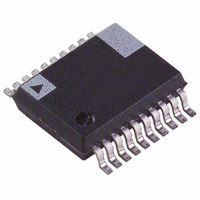
ADE7763ARS Analog Devices Inc, ADE7763ARS Datasheet - Page 13

ADE7763ARS
Manufacturer Part Number
ADE7763ARS
Description
IC ENERGY METER 1PHASE 20SSOP
Manufacturer
Analog Devices Inc
Specifications of ADE7763ARS
Input Impedance
390 KOhm
Measurement Error
0.1%
Voltage - I/o High
2.4V
Voltage - I/o Low
0.8V
Current - Supply
3mA
Voltage - Supply
4.75 V ~ 5.25 V
Operating Temperature
-40°C ~ 85°C
Mounting Type
Surface Mount
Package / Case
20-SSOP (0.200", 5.30mm Width)
Meter Type
Single Phase
For Use With
EVAL-ADE7763ZEB - BOARD EVALUATION FOR ADE7763
Lead Free Status / RoHS Status
Contains lead / RoHS non-compliant
Available stocks
Company
Part Number
Manufacturer
Quantity
Price
Part Number:
ADE7763ARS
Manufacturer:
ADI/亚德诺
Quantity:
20 000
Part Number:
ADE7763ARSZ
Manufacturer:
ADI/亚德诺
Quantity:
20 000
Part Number:
ADE7763ARSZRL
Manufacturer:
ADI/亚德诺
Quantity:
20 000
THEORY OF OPERATION
ANALOG INPUTS
The ADE7763 has two fully differential voltage input channels.
The maximum differential input voltage for input pairs V1P/V1N
and V2P/V2N is ±0.5 V. In addition, the maximum signal level
on analog inputs for V1P/V1N and V2P/V2N is ±0.5 V with
respect to AGND.
Each analog input channel has a programmable gain amplifier
(PGA) with possible gain selections of 1, 2, 4, 8, and 16. The
gain selections are made by writing to the gain register—see
Figure 24. Bits 0 to 2 select the gain for the PGA in Channel 1;
the gain selection for the PGA in Channel 2 is made via Bits 5
to 7. Figure 23 shows how a gain selection for Channel 1 is
made using the gain register.
In addition to the PGA, Channel 1 also has a full-scale input
range selection for the ADC. The ADC analog input range
selection is also made using the gain register—see Figure 24. As
previously mentioned, the maximum differential input voltage
is 0.5 V. However, by using Bits 3 and 4 in the gain register, the
maximum ADC input voltage can be set to 0.5 V, 0.25 V, or
0.125 V. This is achieved by adjusting the ADC reference—see
the Reference Circuit section. Table 5 summarizes the
maximum differential input signal level on Channel 1 for the
various ADC range and gain selections.
CH1OS[7:0]
BITS 0 to 5: SIGN MAGNITUDE CODED OFFSET CORRECTION
BIT 6: NOT USED
BIT 7: DIGITAL INTEGRATOR (ON = 1, OFF = 0; DEFAULT OFF)
7
0
6
0
7
0
5
0
V1P
V
V1N
IN
6
0
4
0
5
0
3
0
GAIN[7:0]
4
0
Figure 23. PGA in Channel 1
2
0
3
0
K × V
1
0
2
0
IN
0
0
1
0
GAIN (K)
SELECTION
0
0
+
OFFSET ADJUST
(±50mV)
Rev. B | Page 13 of 56
Table 5. Maximum Input Signal Levels for Channel 1
Max Signal
Channel 1
0.5 V
0.25 V
0.125 V
0.0625 V
0.0313 V
0.0156 V
0.00781 V
It is also possible to adjust offset errors on Channel 1 and
Channel 2 by writing to the offset correction registers (CH1OS
and CH2OS, respectively). These registers allow channel offsets
in the range ±20 mV to ±50 mV (depending on the gain setting)
to be removed. Note that it is not necessary to perform an offset
correction in an energy measurement application if HPF in
Channel 1 is switched on. Figure 25 shows the effect of offsets
on the real power calculation. As seen from Figure 25, an offset
on Channel 1 and Channel 2 contributes a dc component after
multiplication. Because this dc component is extracted by LPF2
to generate the active (real) power information, the offsets
contribute an error to the active power calculation. This problem
is easily avoided by enabling HPF in Channel 1. By removing
the offset from at least one channel, no error component is
generated at dc by the multiplication. Error terms at cos( ω t) are
removed by LPF2 and by integration of the active power signal
in the active energy register (AENERGY[23:0])—see the Energy
Calculation section.
PGA 2 GAIN SELECT
000 =
001 =
010 =
011 =
100 =
×
×
×
×
×
1
2
4
8
16
CHANNEL 1 AND CHANNEL 2 PGA CONTROL
* REGISTER CONTENTS
SHOW POWER-ON DEFAULTS
7
0
6
0
0.5 V
Gain = 1
Gain = 2
Gain = 4
Gain = 8
Gain = 16
−
−
Figure 24. Analog Gain Register
5
0
GAIN REGISTER*
4
0
ADC Input Range Selection
3
0
2
0
0.25 V
−
Gain = 1
Gain = 2
Gain = 4
Gain = 8
Gain = 16
−
1
0
CHANNEL 1 FULL-SCALE SELECT
00 = 0.5V
01 = 0.25V
10 = 0.125V
0
0
PGA 1 GAIN SELECT
000 =
001 =
010 =
011 =
100 =
ADDR:
0x0A
×
×
×
×
×
1
2
4
8
16
ADE7763
0.125 V
−
−
Gain = 1
Gain = 2
Gain = 4
Gain = 8
Gain = 16


