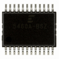
CS5460A-BSZ Cirrus Logic Inc, CS5460A-BSZ Datasheet - Page 40

CS5460A-BSZ
Manufacturer Part Number
CS5460A-BSZ
Description
IC ENERGY METERING 1PHASE 24SSOP
Manufacturer
Cirrus Logic Inc
Datasheet
1.CS5460A-BSZ.pdf
(54 pages)
Specifications of CS5460A-BSZ
Package / Case
24-SSOP
Input Impedance
30 KOhm
Measurement Error
0.1%
Voltage - I/o High
0.8V
Voltage - I/o Low
0.2V
Current - Supply
2.9mA
Voltage - Supply
4.75 V ~ 5.25 V
Operating Temperature
-40°C ~ 85°C
Mounting Type
Surface Mount
Meter Type
Single Phase
Output Voltage Range
2.4 V to 2.6 V
Output Current
1 uA
Input Voltage Range
2.4 V to 2.6 V
Input Current
25 nA
Power Dissipation
500 mW
Operating Temperature Range
- 40 C to + 85 C
Mounting Style
SMD/SMT
Ic Function
Single Phase Bi-directional Power / Energy IC
Brief Features
On-Chip Functions, AC Or DC System Calibration, Power Supply Monitor
Supply Voltage Range
3.3V To 5V
Rohs Compliant
Yes
Lead Free Status / RoHS Status
Lead free / RoHS Compliant
For Use With
CDB5460AU - EVALUATION BOARD FOR CS5460A
Lead Free Status / Rohs Status
Lead free / RoHS Compliant
Other names
598-1094-5
Available stocks
Company
Part Number
Manufacturer
Quantity
Price
Company:
Part Number:
CS5460A-BSZ
Manufacturer:
CIRRUS
Quantity:
2
Company:
Part Number:
CS5460A-BSZR
Manufacturer:
CIRRUS
Quantity:
8 000
Part Number:
CS5460A-BSZR
Manufacturer:
CIRRUS
Quantity:
20 000
4.1.5 Power-Down
The device has two power-down states to conserve power. If the chip is put in stand-by state, all circuitry except the
analog/digital clock generators is turned off. In the sleep state, all circuitry except the digital clock generator and the
instruction decoder is turned off. Waking up the CS5460A out of sleep state requires more time than waking the
device out of stand-by state, because of the extra time needed to re-start and re-stabilize the analog clock signal.
4.1.6 Calibration
The device has the capability of performing a system AC offset calibration, DC offset calibration, AC gain calibration,
and DC gain calibration. Calibration can be done on the voltage channel, the current channel, or both channels at
the same time. Offset and gain calibrations should NOT be performed at the same time (must do one after the oth-
er). For a given application, if DC gain calibrations are performed, then AC gain calibration should not be performed
(and vice-versa). The proper input voltages must be supplied to the device before initiating calibration.
40
[V I]
R
G
O
[S1 S]0
B7
B7
1
1
B6
B6
00 = Reserved
01 = Halt and enter stand-by power saving state. This state allows quick power-on time
10 = Halt and enter sleep power saving state. This state requires a slow power-on time
11 = Reserved
00 = Not allowed
01 = Calibrate the current channel
10 = Calibrate the voltage channel
11 = Calibrate voltage and current channel simultaneously
0 = Normal operation
1 = Perform gain calibration
0 = Normal operation
1 = Perform offset calibration
Power-down state
Specifies AC calibration (R=1) or DC calibration (R=0)
Designates gain calibration
Designates offset calibration
Designates calibration channel
0
1
B5
B5
0
0
B4
B4
S1
V
B3
S0
B3
I
B2
B2
R
0
B1
B1
G
0
CS5460A
DS487F4
B0
B0
O
0


