CS5460A-BSZ Cirrus Logic Inc, CS5460A-BSZ Datasheet - Page 2
CS5460A-BSZ
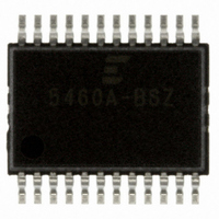
Manufacturer Part Number
CS5460A-BSZ
Description
IC ENERGY METERING 1PHASE 24SSOP
Manufacturer
Cirrus Logic Inc
Datasheet
1.CS5460A-BSZ.pdf
(54 pages)
Specifications of CS5460A-BSZ
Package / Case
24-SSOP
Input Impedance
30 KOhm
Measurement Error
0.1%
Voltage - I/o High
0.8V
Voltage - I/o Low
0.2V
Current - Supply
2.9mA
Voltage - Supply
4.75 V ~ 5.25 V
Operating Temperature
-40°C ~ 85°C
Mounting Type
Surface Mount
Meter Type
Single Phase
Output Voltage Range
2.4 V to 2.6 V
Output Current
1 uA
Input Voltage Range
2.4 V to 2.6 V
Input Current
25 nA
Power Dissipation
500 mW
Operating Temperature Range
- 40 C to + 85 C
Mounting Style
SMD/SMT
Ic Function
Single Phase Bi-directional Power / Energy IC
Brief Features
On-Chip Functions, AC Or DC System Calibration, Power Supply Monitor
Supply Voltage Range
3.3V To 5V
Rohs Compliant
Yes
Lead Free Status / RoHS Status
Lead free / RoHS Compliant
For Use With
CDB5460AU - EVALUATION BOARD FOR CS5460A
Lead Free Status / Rohs Status
Lead free / RoHS Compliant
Other names
598-1094-5
Available stocks
Company
Part Number
Manufacturer
Quantity
Price
Company:

Part Number:
CS5460A-BSZ
Manufacturer:
CIRRUS
Quantity:
2
Company:
Part Number:
CS5460A-BSZR
Manufacturer:
CIRRUS
Quantity:
8 000
Part Number:
CS5460A-BSZR
Manufacturer:
CIRRUS
Quantity:
20 000


TABLE OF CONTENTS
2
1. CHARACTERISTICS AND SPECIFICATIONS ........................................................................ 5
2. OVERVIEW ............................................................................................................................. 12
3. FUNCTIONAL DESCRIPTION ............................................................................................... 21
ANALOG CHARACTERISTICS ................................................................................................ 5
VREFOUT REFERENCE OUTPUT VOLTAGE........................................................................ 7
5V DIGITAL CHARACTERISTICS............................................................................................ 7
3.3 V DIGITAL CHARACTERISTICS........................................................................................ 8
ABSOLUTE MAXIMUM RATINGS ........................................................................................... 8
SWITCHING CHARACTERISTICS .......................................................................................... 9
2.1 Theory of Operation ......................................................................................................... 12
2.2 Performing Measurements ............................................................................................... 13
2.3 Basic Application Circuit Configurations .......................................................................... 16
3.1 Pulse-Rate Output ........................................................................................................... 21
3.2 Pulse Output for Normal Format,
3.3 Auto-Boot Mode Using EEPROM .................................................................................... 24
3.4 Interrupt and Watchdog Timer ......................................................................................... 26
3.5 Oscillator Characteristics ................................................................................................. 27
3.6 Analog Inputs ................................................................................................................... 27
3.7 Voltage Reference ........................................................................................................... 27
3.8 Calibration ........................................................................................................................ 27
2.1.1 DS Modulators ................................................................................................... 12
2.1.2 High-Rate Digital Low-Pass Filters ..................................................................... 12
2.1.3 Digital Compensation Filters ............................................................................... 12
2.1.4 Digital High-Pass Filters ...................................................................................... 12
2.1.5 Overall Filter Response ....................................................................................... 13
2.1.6 Gain and DC Offset Adjustment .......................................................................... 13
2.1.7 Real Energy and RMS Computations ................................................................. 13
2.2.1 CS5460A Linearity Performance ......................................................................... 15
2.2.2 Single Computation Cycle (C=0) ......................................................................... 15
2.2.3 Continuous Computation Cycles (C=1) ............................................................... 16
Stepper Motor Format and Mechanical Counter Format .............................................. 22
3.2.1 Normal Format .................................................................................................... 22
3.2.2 Mechanical Counter Format ................................................................................ 23
3.2.3 Stepper Motor Format ......................................................................................... 23
3.3.1 Auto-Boot Configuration ...................................................................................... 24
3.3.2 Auto-Boot Data for EEPROM .............................................................................. 25
3.3.3 Application Note AN225 ...................................................................................... 26
3.4.1 Interrupt ............................................................................................................... 26
3.4.2 Watch Dog Timer ................................................................................................ 26
3.8.1 Overview of Calibration Process ......................................................................... 27
3.8.2 The Calibration Registers .................................................................................... 28
3.8.3 Calibration Sequence .......................................................................................... 28
3.8.4 Calibration Signal Input Level ............................................................................. 29
3.8.5 Calibration Signal Frequency .............................................................................. 29
3.8.6 Input Configurations for Calibrations ................................................................... 29
3.8.7 Description of Calibration Algorithms .................................................................. 30
3.4.1.1 Clearing the Status Register ............................................................... 26
3.4.1.2 Typical use of the INT pin ................................................................... 26
3.4.1.3 INT Active State .................................................................................. 26
3.4.1.4 Exceptions ........................................................................................... 26
3.8.7.1 AC Offset Calibration Sequence ......................................................... 30
3.8.7.2 DC Offset Calibration Sequence ......................................................... 31
CS5460A
DS487F4
Related parts for CS5460A-BSZ
Image
Part Number
Description
Manufacturer
Datasheet
Request
R

Part Number:
Description:
Driver IC
Manufacturer:
Cirrus Logic Inc
Datasheet:
Part Number:
Description:
IC Sngl-Phs Bi-Directional Power/Energy
Manufacturer:
Cirrus Logic Inc
Datasheet:

Part Number:
Description:
RF COILS < SMD Type: CS Series>
Manufacturer:
SUMIDA [Sumida Corporation]
Datasheet:

Part Number:
Description:
Development Kit
Manufacturer:
Cirrus Logic Inc
Datasheet:
Part Number:
Description:
Development Kit
Manufacturer:
Cirrus Logic Inc
Datasheet:


Part Number:
Description:
High-efficiency PFC + Fluorescent Lamp Driver Reference Design
Manufacturer:
Cirrus Logic Inc
Datasheet:
Part Number:
Description:
Development Kit
Manufacturer:
Cirrus Logic Inc
Datasheet:
Part Number:
Description:
Development Kit
Manufacturer:
Cirrus Logic Inc
Datasheet:

Part Number:
Description:
Development Kit
Manufacturer:
Cirrus Logic Inc
Datasheet:
Part Number:
Description:
Development Kit
Manufacturer:
Cirrus Logic Inc
Datasheet:
Part Number:
Description:
Development Kit
Manufacturer:
Cirrus Logic Inc
Datasheet:
Part Number:
Description:
Development Kit
Manufacturer:
Cirrus Logic Inc
Datasheet:

Part Number:
Description:
Ref Bd For Speakerbar MSA & DSP Products
Manufacturer:
Cirrus Logic Inc