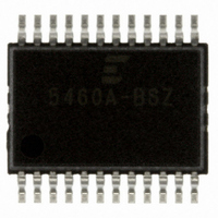
CS5460A-BSZ Cirrus Logic Inc, CS5460A-BSZ Datasheet - Page 12

CS5460A-BSZ
Manufacturer Part Number
CS5460A-BSZ
Description
IC ENERGY METERING 1PHASE 24SSOP
Manufacturer
Cirrus Logic Inc
Datasheet
1.CS5460A-BSZ.pdf
(54 pages)
Specifications of CS5460A-BSZ
Package / Case
24-SSOP
Input Impedance
30 KOhm
Measurement Error
0.1%
Voltage - I/o High
0.8V
Voltage - I/o Low
0.2V
Current - Supply
2.9mA
Voltage - Supply
4.75 V ~ 5.25 V
Operating Temperature
-40°C ~ 85°C
Mounting Type
Surface Mount
Meter Type
Single Phase
Output Voltage Range
2.4 V to 2.6 V
Output Current
1 uA
Input Voltage Range
2.4 V to 2.6 V
Input Current
25 nA
Power Dissipation
500 mW
Operating Temperature Range
- 40 C to + 85 C
Mounting Style
SMD/SMT
Ic Function
Single Phase Bi-directional Power / Energy IC
Brief Features
On-Chip Functions, AC Or DC System Calibration, Power Supply Monitor
Supply Voltage Range
3.3V To 5V
Rohs Compliant
Yes
Lead Free Status / RoHS Status
Lead free / RoHS Compliant
For Use With
CDB5460AU - EVALUATION BOARD FOR CS5460A
Lead Free Status / Rohs Status
Lead free / RoHS Compliant
Other names
598-1094-5
Available stocks
Company
Part Number
Manufacturer
Quantity
Price
Company:
Part Number:
CS5460A-BSZ
Manufacturer:
CIRRUS
Quantity:
2
Company:
Part Number:
CS5460A-BSZR
Manufacturer:
CIRRUS
Quantity:
8 000
Part Number:
CS5460A-BSZR
Manufacturer:
CIRRUS
Quantity:
20 000
2. OVERVIEW
The CS5460A is a CMOS monolithic power mea-
surement device with a real power/energy compu-
tation engine. The CS5460A combines two
programmable gain amplifiers, two ∆Σ modulators,
two high rate filters, system calibration, and
rms/power calculation functions to provide instan-
taneous voltage/current/power data samples as
well as periodic computation results for real (bill-
able) energy, V
modate lower cost metering applications, the
CS5460A can also generate pulse-train signals on
certain output pins, for which the number of pulses
emitted on the pins is proportional to the quantity of
real (billable) energy registered by the device.
The CS5460A is optimized for power measure-
ment applications and is designed to interface to a
shunt or current transformer to measure current,
and to a resistive divider or potential transformer to
measure voltage. To accommodate various input
voltage levels, the current channel includes a pro-
grammable gain amplifier (PGA) which provides
two full-scale input levels, while the voltage chan-
nel’s PGA provides a single input voltage range.
With a single +5 V supply on VA+/-, both of the
CS5460A’s input channels can accomodate com-
mon mode + signal levels between -0.25 V and
VA+.
The CS5460A includes two high-rate digital filters
(one per channel), which decimate/integrate the
output from the 2 ∆Σ modulators. The filters yield
24-bit output data at a (MCLK/K)/1024 output word
rate (OWR). The OWR can be thought of as the ef-
fective sample frequency of the voltage channel and
the current channel.
To facilitate communication to a microcontroller,
the CS5460A includes a simple three-wire serial
interface which is SPI™ and Microwire™ compati-
ble. The serial port has a Schmitt Trigger input on
its SCLK (serial clock) and RESET pins to allow for
slow rise time signals.
2.1 Theory of Operation
A computational flow diagram for the two data
paths is shown in Fig. 3. The reader should refer to
this diagram while reading the following data pro-
cessing
block-by-block.
12
description,
RMS
, and I
RMS
which
. In order to accom-
is
covered
2.1.1 ∆Σ Modulators
The analog waveforms at the voltage/current chan-
nel inputs are subject to the gains of the input
PGAs (not shown in Figure 3). These waveforms
are then sampled by the delta-sigma modulators at
a rate of (MCLK/K)/8 Sps.
2.1.2 High-rate Digital Low-pass Filters
The data is then low-pass filtered, to remove
high-frequency noise from the modulator output.
Referring to Figure 3, the high rate filter on the volt-
age channel is implemented as a fixed Sinc
The current channel uses a Sinc
lows the current channel to make accurate mea-
surements over a wider span of the total input
range, in comparison to the accuracy range of the
voltage channel. (This subject is discussed more in
Section 2.2.1)
Also note from Figure 3 that the digital data on the
voltage channel is subjected to a variable time-de-
lay filter. The amount of delay depends on the val-
ue of the seven phase compensation bits (see
Phase Compensation). Note that when the phase
compensation bits PC[6:0] are set to their default
setting of “0000000” (and if MCLK/K = 4.096 MHz)
then the nominal time delay that is imposed on the
original analog voltage input signal, with respect to
the original analog current input signal, is ~1.0
This translates into a delay of ~0.0216 degrees at
60 Hz.
2.1.3 Digital Compensation Filters
The data from both channels is then passed
through two FIR compensation filters, whose pur-
pose is to compensate for the magnitude roll-off of
the low-pass filtering operation (mentioned earli-
er).
2.1.4 Digital High-pass Filters
Both channels provide an optional high-pass filter
(denoted as “HPF” in Figure 3) which can be en-
gaged into the signal path, to remove the DC con-
tent from the current/voltage signal before the
RMS/energy calculations are made. These filters
are activated by enabling certain bits in the Config-
uration Register.
If the high-pass filter is engaged in only one of the
two channels, then the all-pass filter (see “APF” in
4
filter, which al-
CS5460A
DS487F4
2
filter.
µ
s.


