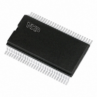
PCF8576T/1,112 NXP Semiconductors, PCF8576T/1,112 Datasheet - Page 19

PCF8576T/1,112
Manufacturer Part Number
PCF8576T/1,112
Description
IC LCD DRV UNVRSL LOW-MUX 56VSOP
Manufacturer
NXP Semiconductors
Datasheet
1.PCF8576T1112.pdf
(44 pages)
Specifications of PCF8576T/1,112
Package / Case
56-VSOP
Mounting Type
Surface Mount
Current - Supply
180µA
Voltage - Supply
2 V ~ 9 V
Operating Temperature
-40°C ~ 85°C
Interface
I²C
Display Type
LCD
Configuration
40 Segment
Lead Free Status / RoHS Status
Lead free / RoHS Compliant
Digits Or Characters
-
Lead Free Status / Rohs Status
Details
Other names
933804620112::PCF8576T/1::PCF8576T/1
Philips Semiconductors
7
The I
between different ICs or modules. The two lines are a
serial data line (SDA) and a serial clock line (SCL). Both
lines must be connected to a positive supply via a pull-up
resistor when connected to the output stages of a device.
Data transfer may be initiated only when the bus is not
busy.
7.1
One data bit is transferred during each clock pulse. The
data on the SDA line must remain stable during the HIGH
period of the clock pulse as changes in the data line at this
time will be interpreted as a control signal.
7.2
Both data and clock lines remain HIGH when the bus is not
busy. A HIGH-to-LOW transition of the data line, while the
clock is HIGH is defined as the START condition (S). A
LOW-to-HIGH transition of the data line while the clock is
HIGH is defined as the STOP condition (P).
7.3
A device generating a message is a ‘transmitter’, a device
receiving a message is the ‘receiver’. The device that
controls the message is the ‘master’ and the devices which
are controlled by the master are the ‘slaves’.
7.4
The number of data bytes transferred between the START
and STOP conditions from transmitter to receiver is
unlimited. Each byte of eight bits is followed by an
acknowledge bit. The acknowledge bit is a HIGH level
signal put on the bus by the transmitter during which time
the master generates an extra acknowledge related clock
pulse. A slave receiver which is addressed must generate
an acknowledge after the reception of each byte. Also a
master receiver must generate an acknowledge after the
reception of each byte that has been clocked out of the
slave transmitter. The device that acknowledges must
pull-down the SDA line during the acknowledge clock
pulse, so that the SDA line is stable LOW during the HIGH
period of the acknowledge related clock pulse (set-up and
hold times must be taken into consideration). A master
receiver must signal an end of data to the transmitter by
not generating an acknowledge on the last byte that has
been clocked out of the slave. In this event the transmitter
must leave the data line HIGH to enable the master to
generate a STOP condition.
2001 Oct 02
Universal LCD driver for low multiplex rates
CHARACTERISTICS OF THE I
2
C-bus is for bidirectional, two-line communication
Bit transfer (see Fig.12)
START and STOP conditions (see Fig.13)
System configuration (see Fig.14)
Acknowledge (see Fig.15)
2
C-BUS
19
7.5
The PCF8576 acts as an I
not initiate I
master receiver. The only data output from the PCF8576
are the acknowledge signals of the selected devices.
Device selection depends on the I
on the transferred command data and on the hardware
subaddress.
In single device application, the hardware subaddress
inputs A0, A1 and A2 are normally connected to V
defines the hardware subaddress 0. In multiple device
applications A0, A1 and A2 are connected to V
accordance with a binary coding scheme such that no two
devices with a common I
same hardware subaddress.
In the power-saving mode it is possible that the PCF8576
is not able to keep up with the highest transmission rates
when large amounts of display data are transmitted. If this
situation occurs, the PCF8576 forces the SCL line to LOW
until its internal operations are completed. This is known
as the ‘clock synchronization feature’ of the I
serves to slow down fast transmitters. Data loss does not
occur.
7.6
To enhance noise immunity in electrically adverse
environments, RC low-pass filters are provided on the
SDA and SCL lines.
7.7
Two I
reserved for the PCF8576. The least significant bit of the
slave address that a PCF8576 will respond to is defined by
the level connected at its input pin SA0. Therefore, two
types of PCF8576 can be distinguished on the same
I
The I
initiated with a START condition (S) from the I
master which is followed by one of the two PCF8576 slave
addresses available. All PCF8576s with the corresponding
SA0 level acknowledge in parallel with the slave address
but all PCF8576s with the alternative SA0 level ignore the
whole I
2
C-bus which allows:
Up to 16 PCF8576s on the same I
LCD applications
The use of two types of LCD multiplex on the same
I
2
C-bus.
2
2
C-bus protocol is shown in Fig.16. The sequence is
C-bus slave addresses (0111000 and 0111001) are
PCF8576 I
Input filters
I
2
2
C-bus transfer.
C-bus protocol
2
C-bus transfers or transmit data to an I
2
C-bus controller
2
C-bus slave address have the
2
C-bus slave receiver. It does
2
C-bus slave address,
2
Product specification
C-bus for very large
PCF8576
2
C-bus and
SS
2
C-bus
or V
SS
2
C-bus
which
DD
in


