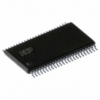
PCF8562TT/2,118 NXP Semiconductors, PCF8562TT/2,118 Datasheet - Page 20

PCF8562TT/2,118
Manufacturer Part Number
PCF8562TT/2,118
Description
IC LCD DRIVER 32/128SEG 48-TSSOP
Manufacturer
NXP Semiconductors
Datasheet
1.PCF8562TT2118.pdf
(37 pages)
Specifications of PCF8562TT/2,118
Package / Case
48-TSSOP
Display Type
LCD
Configuration
7 Segment + DP, 14 Segment (32 Segment)
Interface
I²C
Current - Supply
32µA
Voltage - Supply
1.8 V ~ 5.5 V
Operating Temperature
-40°C ~ 85°C
Mounting Type
Surface Mount
Number Of Digits
16
Number Of Segments
32
Maximum Clock Frequency
2640 Hz
Operating Supply Voltage
1.8 V to 5.5 V
Maximum Power Dissipation
400 mW
Maximum Operating Temperature
+ 85 C
Attached Touch Screen
No
Maximum Supply Current
20 uA
Minimum Operating Temperature
- 40 C
Lead Free Status / RoHS Status
Lead free / RoHS Compliant
For Use With
OM6292 - DEMO BOARD PCA2125 RTCOM10088 - KIT FOR LCD DEMO LPC900622-1003 - KIT FOR LCD DEMO
Digits Or Characters
-
Lead Free Status / Rohs Status
Lead free / RoHS Compliant
Other names
568-2029-2
PCF8562TT/2,518
PCF8562TT/2-T
PCF8562TT/2,518
PCF8562TT/2-T
NXP Semiconductors
PCF8562_5
Product data sheet
7.16.4 Acknowledge
7.16.5 I
The number of data bytes that can be transferred from transmitter to receiver between the
START and STOP conditions is unlimited. Each byte of eight bits is followed by an
acknowledge bit. The acknowledge bit is a HIGH-level signal on the bus that is asserted
by the transmitter during which time the master generates an extra acknowledge related
clock pulse. An addressed slave receiver must generate an acknowledge after receiving
each byte. Also a master receiver must generate an acknowledge after receiving each
byte that has been clocked out of the slave transmitter. The acknowledging device must
pull-down the SDA line during the acknowledge clock pulse so that the SDA line is stable
LOW during the HIGH period of the acknowledge related clock pulse (set-up and hold
times must be taken into consideration). A master receiver must signal an end of data to
the transmitter by not generating an acknowledge on the last byte that has been clocked
out of the slave. In this event the transmitter must leave the data line HIGH to enable the
master to generate a STOP condition (see
The PCF8562 acts as an I
transmit data to an I
the acknowledge signals of the selected devices. Device selection depends on the
I
subaddress.
2
2
Fig 13. System configuration
Fig 14. Acknowledgement of the I
C-bus slave address, on the transferred command data and on the hardware
C-bus controller
SCL
SDA
by transmitter
data output
by receiver
data output
TRANSMITTER/
SCL from
RECEIVER
master
MASTER
All information provided in this document is subject to legal disclaimers.
2
condition
START
C-bus master receiver. The only data output from the PCF8562 are
S
Rev. 05 — 19 May 2010
2
RECEIVER
C-bus slave receiver. It does not initiate I
SLAVE
2
1
C-bus
TRANSMITTER/
RECEIVER
Universal LCD driver for low multiplex rates
Figure
SLAVE
2
14).
TRANSMITTER
MASTER
not acknowledge
acknowledge
8
2
acknowledgement
C-bus transfers or
clock pulse for
PCF8562
TRANSMITTER/
© NXP B.V. 2010. All rights reserved.
RECEIVER
MASTER
9
mbc602
mga807
20 of 37


