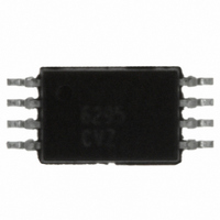
ISL6295CVZ Intersil, ISL6295CVZ Datasheet - Page 19

ISL6295CVZ
Manufacturer Part Number
ISL6295CVZ
Description
IC FUEL GAUGE LOW VOLTAGE8-TSSOP
Manufacturer
Intersil
Datasheet
1.ISL6295CVZ.pdf
(25 pages)
Specifications of ISL6295CVZ
Function
Fuel, Gas Gauge/Monitor
Battery Type
Lithium-Ion (Li-Ion), Lithium-Polymer (Li-Pol)
Voltage - Supply
2.8 V ~ 7 V
Operating Temperature
-20°C ~ 85°C
Mounting Type
Surface Mount
Package / Case
8-TSSOP
Battery Management Function
Fuel Gauge
Supply Voltage Range
2.8V To 7V
Interface Type
2-Wire, Serial, I2C
Battery Ic Case Style
TSSOP
No. Of Pins
8
Rohs Compliant
Yes
Lead Free Status / RoHS Status
Lead free / RoHS Compliant
Available stocks
Company
Part Number
Manufacturer
Quantity
Price
Company:
Part Number:
ISL6295CVZ
Manufacturer:
Intersil
Quantity:
40
Company:
Part Number:
ISL6295CVZ
Manufacturer:
INTERSIL
Quantity:
17
Part Number:
ISL6295CVZ
Manufacturer:
INTERSIL
Quantity:
20 000
PP0
OE0
IE1
IE0
OUT1
OUT0
The eight A/D result registers contain the following:
Magnitude Magnitude of A/D output: Reports the
Sign
GPIO CONTROL REGISTER - GPIOctrl
(Address 53 Hex/83 Decimal)
These GPIO control bits are relevent only when the
respective GPIO enable bit (contained within the VREFT
register) is set.
PP0
7
OE0
6
IO0 Push-Pull Output mode: Setting this bit to
‘1’ will configure the IO0 pin as a push-pull digital
output. If set to ‘0’, the IO0 pin will become an
open drain output with a 300k Ω pull-up to the
internal regulated supply. To be used in
conjunction with the “OE0” bit.
IO0 Output Enable: Setting this bit to ‘1’ will
configure the IO0 pin to be either a push-pull
output (when PP0 = ’1’) or open drain output
(when PP0 = ‘0’). If “OE0” is reset to ‘0’, the IO0
pin is three-stated (when PP0 = ‘1’) or pulled up
to the internal regulated supply through a 300k Ω
resistor (when PP0 = ‘0’).
IO1 Input enable: Setting this bit to ‘1’ enables
the IO1 pin to be used as a digital input. If reset
to ‘0’, the digital input buffer on IO1 is powered
down and the “IN1” bit will always read logic 0.
IO0 Input enable: Setting this bit to ‘1’ enables
the IO0 pin to be used as a digital input. If reset
to ‘0’, the digital input buffer on IO0 is powered
down and the “IN0” bit will always read logic 0.
IO1 Output Data: Controls the open drain pull-
down device. When “0” is written, the pull-down
device is enabled and the IO1 pin outputs a logic
0. When set to “1”, the pull-down device is
disabled and the IO1 is three-stated.
IO0 Output Data: Sets the logic level driven on
the IO0 pin. Relevant only when Output Enable
bit “OE0” is set.
magnitude value of the A/D measurement with
00h representing a zero value and 7Fh
representing full scale (magnitude of ADC input
voltage equals V
left-justified, meaning that result from a N-bit
conversion, as defined by the resolution
specified within the A/D Control register, will
occupy bit locations from bit 14 to bit (15-N).
Polarity of the A/D measurement: The sign bit
shows the polarity of the A/D measurement.
0 = positive value
1 = negative value
IE1
5
IE0
4
19
REF
OUT1
3
). The magnitude value is
OUT0
2
IN1
1
IN0
0
ISL6295
IN1
IN0
ACCUMULATOR CLEAR REGISTER - ACCclr
(Address - 62 Hex/98 Decimal)
A ‘1’ in any of the “CLRn” bits will clear the associated
accumulator. Following the clear operation, all of the bits in
the AccClr register will be reset to 0.
CLR7
CLR6
CLR5
CLR4
CLR3
CLR2
CLR1
CLR0
TRIP POINT VALUE REGISTERS
There are 5 registers that are utilized to set up Trip Point
Values. These registers are used when enabled by the
TRIPctrl register to enter or exit various power modes. Three
of these trip point value registers contain voltage values and
two contain current values. Locations of the trip point
detection enable bit and the corresponding compare and trip
point value registers are listed below:
VPtrip, VCtrip and SStrip are used as voltage values to be
compared to VPres, GPADres and VPres respectively for
transitioning in and out of various power modes. I+trip and
I-trip are used as current values to be compared to Ires for
transitioning in and out of various power modes. The data
format in these registers is left justified. For the purpose of
trip point detection, only magnitude is compared and the sign
is ignored.
I+trip
I-trip
VPtrip
VCtrip
SStrip
CLR7
REGISTER
Sign
7
15
TPV
CLR6
14 13 12 11 10 9
6
Clear GPADT Timer
Clear GPADA Accumulator
Clear TAT Timer
Clear TA Accumulator
Clear CTC Timer
Clear CCA Accumulator
Clear DTC Timer
Clear DCA Accumulator
IO1 Input Data: Current logic state of the IO1
pin (read- only).
IO0 Input Data: Current logic state of the IO0
pin (read- only).
CLR5
LOCATION
5
6Ch
60h
64h
68h
70h
CLR4
4
Magnitude
8
CLR3
VPres or GPADres
COMPARISON
3
7
REGISTER
VPres
VPres
6
Ires
Ires
CLR2
2
5
4
CLR1
1
3
February 8, 2011
ENABLE
GPADent
VPent or
2
Shent
VPex
Ient
BIT
Iex
FN9074.2
CLR0
1
0
0


