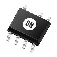
NCP1219AD65R2G ON Semiconductor, NCP1219AD65R2G Datasheet - Page 6

NCP1219AD65R2G
Manufacturer Part Number
NCP1219AD65R2G
Description
IC CTRLR PWM CM OVP OTP HV 7SOIC
Manufacturer
ON Semiconductor
Datasheet
1.NCP1219AD100R2G.pdf
(20 pages)
Specifications of NCP1219AD65R2G
Output Isolation
Isolated
Frequency Range
61.8 ~ 68.3kHz
Voltage - Input
9 ~ 20 V
Power (watts)
920mW
Operating Temperature
-40°C ~ 150°C
Package / Case
8-SOIC (0.154", 3.90mm Width) 7 leads
Number Of Outputs
1
Duty Cycle (max)
80 %
Output Voltage
- 0.3 V to + 20 V
Output Current
800 mA
Mounting Style
SMD/SMT
Switching Frequency
68.25 KHz
Maximum Operating Temperature
+ 150 C
Fall Time
20 ns
Minimum Operating Temperature
- 40 C
Rise Time
30 ns
Synchronous Pin
No
Topology
Flyback
Lead Free Status / RoHS Status
Lead free / RoHS Compliant
Available stocks
Company
Part Number
Manufacturer
Quantity
Price
Company:
Part Number:
NCP1219AD65R2G
Manufacturer:
ON Semiconductor
Quantity:
165
Table 3. ELECTRICAL CHARACTERISTICS
0.1 mF, for typical values T
5. Guaranteed by the I
6. Guaranteed by design only.
STARTUP AND SUPPLY CIRCUITS
CURRENT SENSE
FEEDBACK INPUT
SOFT−START
OSCILLATOR
Supply Voltage
UVLO Filter Delay
Inhibit Threshold Voltage
Inhibit Bias Current
Minimum Startup Voltage
Startup Current
Startup Circuit Reverse Current
Off−State Leakage Current
Breakdown Voltage (Note 5)
Supply Current
Current Sense Voltage Threshold
Leading Edge Blanking Duration
Propagation Delay
Ramp Compensation Peak Current
Ramp Compensation Valley Current
Open Feedback Voltage
Internal Pull−up Resistance
Feedback Pull−up Current
Feedback to Current Set Point Ratio
Soft−Start Period
Oscillator Frequency
Frequency Modulation in
Percentage of f
Frequency Modulation Period
Maximum Duty Ratio
Startup Threshold
Minimum Operating Voltage
Undervoltage Lockout
Double Hiccup Threshold
Logic Reset Voltage
Device Disabled/Fault
Device Enabled/No Switching
Device Switching (65 kHz)
Device Switching (100 kHz)
65 kHz Option
100 kHz Option
Characteristics
OSC
HV(off)
J
= 25°C, for min/max values, T
test.
I
start
V
V
V
Skip/latch
Skip/latch
CS
V
Apply voltage step on CS pin
V
= 0.5 mA, V
Skip/latch
Skip/latch
V
> V
V
V
Measured at 0.9 V
HV
T
T
T
T
CC
HV
J
J
ILIM
(V
J
J
V
V
V
V
C
V
I
= 500 V, V
= −40_C to 125_C
= −40_C to 125_C
inhibit
= open, C
= open, C
= −40_C to 85_C
= −40_C to 85_C
CC
CC
CC
CC
= V
= 0 V, V
DRV
HV
CC
Conditions
I
V
HV
T
T
V
to 50% DRV turns off,
= 5.2 V, V
= open, V
J
J
CC
J
Decreasing
Decreasing
Decreasing
Decreasing
FB
= 60 V, V
CC (on)
Increasing
http://onsemi.com
= 25_C
= 25_C
= 50 mA
= 1000 pF
is –40°C to 125°C, unless otherwise noted)
CC
= 500 mA
= 0 V
= 0 V
= V
CC
CC
DRV
DRV
– 0.5 V
= 14 V
CC(on)
FB
= 14 V
FB
CC
= 1000 pF
= 1000 pF
ILIM
= open
6
= 0 V
= 11.3 V, V
– 0.5 V
FB
= 2 V, V
t
V
I
I
UVLO(delay)
I
V
V
HV(reverse)
ramp(valley)
V
V
ramp(peak)
Symbol
CC(hiccup)
V
t
V
CC(reset)
V
start(min)
I
SSTART
UVLO
FB(open)
CC(MIN)
I
HV(off)
I
I
V
t
BR(DS)
f
CC(on)
inhibit
I
I
I
CC3A
CC3B
I
t
R
delay
inhibit
OSC
start
CC1
CC2
LEB
I
ratio
ILIM
FB
D
FB
Skip/latch
= 0 V, V
61.75
11.2
0.35
0.95
Min
100
500
100
141
9.0
8.4
4.9
5.5
3.2
58
55
95
89
85
75
–
–
–
–
–
–
–
–
–
–
–
–
–
–
–
–
–
CS
= 0 V, V
12.7
0.67
12.8
16.7
±7.5
Typ
200
184
100
280
100
9.9
9.4
5.7
4.0
0.6
1.4
2.2
2.4
1.0
3.6
3.0
4.8
6.0
50
20
12
59
65
80
–
–
0
–
–
–
–
DRV
68.25
= open, C
Max
13.8
10.8
10.6
0.90
18.5
1.05
350
100
330
150
392
105
107
107
6.3
0.8
2.1
2.7
3.2
3.9
28
50
71
71
85
–
–
–
–
–
–
–
–
–
–
CC
Unit
kHz
mA
mA
mA
mA
mA
mA
mA
kW
mA
ms
ms
ms
ns
ns
%
%
V
V
V
V
V
V
=


