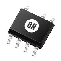
NCP1219AD65R2G ON Semiconductor, NCP1219AD65R2G Datasheet - Page 4

NCP1219AD65R2G
Manufacturer Part Number
NCP1219AD65R2G
Description
IC CTRLR PWM CM OVP OTP HV 7SOIC
Manufacturer
ON Semiconductor
Datasheet
1.NCP1219AD100R2G.pdf
(20 pages)
Specifications of NCP1219AD65R2G
Output Isolation
Isolated
Frequency Range
61.8 ~ 68.3kHz
Voltage - Input
9 ~ 20 V
Power (watts)
920mW
Operating Temperature
-40°C ~ 150°C
Package / Case
8-SOIC (0.154", 3.90mm Width) 7 leads
Number Of Outputs
1
Duty Cycle (max)
80 %
Output Voltage
- 0.3 V to + 20 V
Output Current
800 mA
Mounting Style
SMD/SMT
Switching Frequency
68.25 KHz
Maximum Operating Temperature
+ 150 C
Fall Time
20 ns
Minimum Operating Temperature
- 40 C
Rise Time
30 ns
Synchronous Pin
No
Topology
Flyback
Lead Free Status / RoHS Status
Lead free / RoHS Compliant
Available stocks
Company
Part Number
Manufacturer
Quantity
Price
Company:
Part Number:
NCP1219AD65R2G
Manufacturer:
ON Semiconductor
Quantity:
165
Table 1. PIN FUNCTION DESCRIPTION
Pin
1
2
3
4
5
6
8
Skip/latch
Name
GND
DRV
VCC
FB
CS
HV
This pin provides a latch input to permanently disable the device under a fault condition. It also allows the user to
adjust the skip threshold. A resistor between this pin and GND provides noise immunity to the latch input and sets
the skip threshold. The voltage on this pin is determined by the combination of the internal voltage divider and the
external resistor to ground. The default skip threshold is 1.1 V (typical) if no external resistor is used. An internal
clamp prevents the skip level from increasing above 1.3 V if the Skip/latch pin is pulled high to latch the controller.
The voltage on this pin is proportional to the output load on the converter. An internal resistor divider sets the
voltage on this pin above the regulation threshold (3 V) and an external optocoupler pulls the pin low to achieve
regulation. While the FB voltage is above its regulation threshold, the overload timer is enabled. If the overload
timer expires, the controller enters a double hiccup mode (option B) or is latched (option A) depending on the ver-
sion of the device. The converter enters skip mode if the FB voltage is below the skip threshold.
A voltage ramp proportional to the primary current is applied to this pin. The maximum current is reached once the
ramp voltage reaches 1 V (typical). A 100 mA (typical) current source provides ramp compensation. The amount of
ramp compensation is adjusted with a series resistor between the CS pin and the current sense resistor.
Analog ground.
Main output of the PWM Controller. DRV has a source resistance of 12.6 W (typical) and a sink resistance of 6.7 W
(typical).
Positive input supply. This pin connects to an external capacitor for energy storage. An internal current source
supplies current from the HV pin to this pin. Once the V
source turns off and the DRV is enabled. The current source turns on once V
This mode of operation is known as dynamic self supply (DSS).
If the bias current consumption exceeds the startup current, and V
verter turns off and enters a double hiccup mode. If the V
reduced to 200 mA (typical), reducing power dissipation.
This is the input of the high voltage startup regulator and connects directly to the bulk voltage. A controlled current
source supplies current from this pin to the V
charge current is 12.8 mA (typical).
http://onsemi.com
CC
4
capacitor, eliminating the need for an external startup resistor. The
Description
CC
CC
voltage reaches V
voltage is below 0.67 V (typical) the startup current is
CC
drops 0.5 V (typical) below V
CC(on)
CC
falls to V
(12.7 V typical), the current
CC(min)
(9.9 V typical).
CC(min)
the con-


