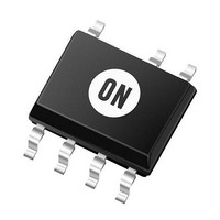
NCP1219AD65R2G ON Semiconductor, NCP1219AD65R2G Datasheet - Page 5

NCP1219AD65R2G
Manufacturer Part Number
NCP1219AD65R2G
Description
IC CTRLR PWM CM OVP OTP HV 7SOIC
Manufacturer
ON Semiconductor
Datasheet
1.NCP1219AD100R2G.pdf
(20 pages)
Specifications of NCP1219AD65R2G
Output Isolation
Isolated
Frequency Range
61.8 ~ 68.3kHz
Voltage - Input
9 ~ 20 V
Power (watts)
920mW
Operating Temperature
-40°C ~ 150°C
Package / Case
8-SOIC (0.154", 3.90mm Width) 7 leads
Number Of Outputs
1
Duty Cycle (max)
80 %
Output Voltage
- 0.3 V to + 20 V
Output Current
800 mA
Mounting Style
SMD/SMT
Switching Frequency
68.25 KHz
Maximum Operating Temperature
+ 150 C
Fall Time
20 ns
Minimum Operating Temperature
- 40 C
Rise Time
30 ns
Synchronous Pin
No
Topology
Flyback
Lead Free Status / RoHS Status
Lead free / RoHS Compliant
Available stocks
Company
Part Number
Manufacturer
Quantity
Price
Company:
Part Number:
NCP1219AD65R2G
Manufacturer:
ON Semiconductor
Quantity:
165
Stresses exceeding Maximum Ratings may damage the device. Maximum Ratings are stress ratings only. Functional operation above the
Recommended Operating Conditions is not implied. Extended exposure to stresses above the Recommended Operating Conditions may affect
device reliability.
1. This device series contains ESD protection and exceeds the following tests:
2. This device contains Latch−Up protection and exceeds ±100 mA per JEDEC Standard JESD78.
3. As mounted on a 40x40x1.5 mm FR4 substrate with a single layer of 80 mm
4. As mounted on a 40x40x1.5 mm FR4 substrate with a single layer of 650 mm
Table 2. MAXIMUM RATINGS
HV Voltage
HV Current
Supply Voltage
Supply Current
Skip/latch Voltage
Skip/latch Current
FB Voltage
FB Current
CS Voltage
CS Current
DRV Voltage
DRV Current
Operating Junction Temperature
Storage Temperature Range
Power Dissipation (T
Thermal Resistance, Junction to Ambient (2.0 Oz Cu Printed Circuit Copper Clad)
a JEDEC 51 low conductivity test PCB. Test conditions were under natural convection or zero air flow.
for a JEDEC 51 high conductivity test PCB. Test conditions were under natural convection or zero air flow.
D Suffix, Plastic Package Case 751U (SOIC−7) (Note 4)
D Suffix, Plastic Package Case 751U (SOIC−7)
Pins 1– 6: Human Body Model 3000 V per JEDEC JESD22−A114−F .
Pins 1– 6:
Pin 8 is the HV startup of the device and is rated to the maximum rating of the part, or 500 V.
Junction to Air, Low conductivity PCB (Note 3)
Junction to Lead, Low conductivity PCB (Note 3)
Junction to Air, High conductivity PCB (Note 4)
Junction to Lead, High conductivity PCB (Note 4)
Machine Model Method 300 V per JEDEC JESD22−A115−A.
A
= 25°C, 2.0 Oz Cu, 1.0 Sq Inch Printed Circuit Copper Clad)
(Notes 1 − 4)
Rating
http://onsemi.com
5
2
of 2 oz copper traces and heat spreading area. As specified for
2
of 2 oz copper traces and heat spreading area. As specified
V
I
Symbol
Skip/latch
Skip/latch
V
R
R
R
R
I
V
V
V
V
T
I
DRV
I
I
I
P
DRV
T
HV
CC
CS
FB
θJA
θJA
stg
θJL
θJL
HV
CC
CS
FB
D
J
−500 to 800
−0.3 to 500
−0.3 to 9.5
−0.3 to 5.0
−0.3 to 5.0
–40 to 150
–60 to 150
−0.3 to 20
−0.3 to 20
Value
0.92
100
100
100
100
100
177
136
75
69
°C/W
Unit
mA
mA
mA
mA
mA
mA
°C
°C
W
V
V
V
V
V
V


