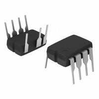
NCP1377PG ON Semiconductor, NCP1377PG Datasheet - Page 8

NCP1377PG
Manufacturer Part Number
NCP1377PG
Description
IC CTRLR PWM CM OVP UVLO 8DIP
Manufacturer
ON Semiconductor
Datasheet
1.NCP1377BPG.pdf
(17 pages)
Specifications of NCP1377PG
Output Isolation
Isolated
Frequency Range
100kHz
Voltage - Input
8.2 ~ 18 V
Operating Temperature
0°C ~ 125°C
Package / Case
8-DIP (0.300", 7.62mm), 7 Leads
Number Of Outputs
1
Output Voltage
18 V
Output Current
500 mA
Mounting Style
Through Hole
Switching Frequency
100 KHz
Maximum Operating Temperature
+ 150 C
Fall Time
20 ns
Rise Time
40 ns
Synchronous Pin
No
Topology
Flyback
Lead Free Status / RoHS Status
Lead free / RoHS Compliant
Other names
NCP1377PGOS
Available stocks
Company
Part Number
Manufacturer
Quantity
Price
Part Number:
NCP1377PG
Manufacturer:
ON/安森美
Quantity:
20 000
constrained below 16 V, which is the maximum rating on
pin 6. Figure 17 portrays a typical NCP1377 startup
sequence with a Vcc regulated at 12.5 V.
inserted between the current sense input and the sense
element. Everytime the NCP1377 output driver goes low,
a 200 mA source forces a current to flow through the sense
pin (Figure 19): when the driver is high, the current source
is off and the current sense information is normally
processed. As soon as the driver goes low, the current
source delivers 200 mA and develops a ground referenced
voltage across Rskip. If this voltage is below the feedback
voltage, the current sense comparator stays in the low state
and the internal latch can be triggered by the next clock
cycle. Now, if because of a low load mode the feedback
Once the power supply has started, the V
The skip level selection is done through a simple resistor
13.5
12.5
10.5
9.50
11.5
Figure 18. The Skip Cycle Takes Place at Low Peak
300
200
100
Currents which Guarantees Noise−Free Operation
0
RECURRENCE
Figure 17. A Typical Startup Sequence
12.5 V
MAX PEAK
CURRENT
WIDTH
for the NCP1377
NORMAL CURRENT
MODE OPERATION
CURRENT LIMIT
SKIP CYCLE
Regulation
CC
shall be
http://onsemi.com
8
Skipping Cycle Mode
when the output power demand drops below a given level.
This is accomplished by monitoring the FB pin. In normal
operation, pin 2 imposes a peak current accordingly to the
load value. If the load demand decreases, the internal loop
asks for less peak current. When this setpoint reaches a
determined level, the IC prevents the current from
decreasing further down and starts to blank the output
pulses: the IC enters the so−called skip cycle mode, also
named controlled burst operation. The power transfer now
depends upon the width of the pulse bunches (Figure 18)
and
Lp = Primary inductance
Fsw = Switching frequency within the burst
Ip = Peak current at which skip cycle occurs
D
voltage is below Rskip level, then the current sense
comparator permanently resets the latch and the next clock
cycle (given by the demagnetization detection) is ignored:
we are skipping cycles as shown by Figure 18. As soon as
the feedback voltage goes up again, there can be two
situations: the recurrent period is small and a new
demagnetization detection (next wave) signal triggers the
NCP1377. To the opposite, in low output power conditions,
no more ringing waves are present on the drain and the
toggling of the current sense comparator alone initiates a
new cycle start. Figure 20 depicts these two different
situations.
1
2
burst
The NCP1377 automatically skips switching cycles
RESET
· Lp · Ip 2 · Fsw · D burst
Level Selection via a Series Resistor Inserted in
Figure 19. A Patented Method Allows for Skip
= Burst width/burst recurrence
follows
+
Series with the Current
-
+
the
3
2
DRIVER
with:
DRIVER = HIGH ? I = 0
DRIVER = LOW ? I = 200 mA
following
R
skip
R
formula:
sense


