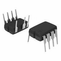
NCP1377PG ON Semiconductor, NCP1377PG Datasheet

NCP1377PG
Specifications of NCP1377PG
Available stocks
Related parts for NCP1377PG
NCP1377PG Summary of contents
Page 1
NCP1377, NCP1377B PWM Current-Mode Controller for Free-Running Quasi-Resonant Operation The NCP1377 combines a true current mode modulator and a demagnetization detector which ensures full borderline/critical Conduction Mode in any load/line conditions together with minimum drain voltage switching (Quasi−Resonant operation). Due ...
Page 2
OVP and + Demag Universal Network *Please refer to the application information section. PIN FUNCTION DESCRIPTION Pin Symbol Function 1 Demag Core reset detection and OVP 2 FB Sets the peak current setpoint 3 CS Current sense input and skip ...
Page 3
HV PON 12.5 V 7.5 V 5.6 V (Fault) Fault To Internal Mngt. Supply GND MAXIMUM RATINGS Continuous Power Supply or Drive Voltage Transient Power Supply Voltage, Duration < 10 ms, I ...
Page 4
ELECTRICAL CHARACTERISTICS (For typical values T = 25°C, for min/max values T J Characteristic SUPPLY SECTION V Increasing Level at which the Current Source Turns−Off CC Minimum Operating Voltage after Turn−On V Decreasing Level at which the Latchoff Phase Ends ...
Page 5
TEMPERATURE (°C) Figure 3. V Threshold versus Temperature CCON 1.60 1.40 1.20 1.00 0.80 0.60 0.40 −50 −30 − TEMPERATURE (°C) Figure 5. Current ...
Page 6
TEMPERATURE (°C) Figure 9. Drive Source Resistance versus Temperature 120 100 −50 −30 − TEMPERATURE (°C) Figure ...
Page 7
TEMPERATURE (°C) Figure 15. DMG Pin Internal Resistance versus Temperature APPLICATION INFORMATION INTRODUCTION The NCP1377 implements a standard current mode architecture where the switch−off time is dictated ...
Page 8
Once the power supply has started, the V constrained below 16 V, which is the maximum rating on pin 6. Figure 17 portrays a typical NCP1377 startup sequence with a Vcc regulated at 12.5 V. 13.5 12.5 V 12.5 11.5 ...
Page 9
Drain Signal Timeout Signal Drain Signal Timeout Signal Figure 20. When the primary natural ringing becomes too low, the internal TimeOut together with the sense comparator initiates a new cycle when FB passes the skip level. An optocoupler is generally ...
Page 10
An internal timer prevents any restart within 8.0 ms further to the driver going−low transition for NCP1377, and 3.0 ms for NCP1377B. This prevents the switching frequency to exceed (1.0 blank leakage inductance tripping at turn−off. In ...
Page 11
Thermistor Rdem Figure 25. A simple arrangement triggers the latchoff as soon as the temperature exceeds a given setpoint. Shutting Off the NCP1377 Shutdown can easily be implemented through a simple ...
Page 12
Vcc ON Figure 28. Typical Waveforms in Short Circuit Conditions Soft−Start The NCP1377 features an internal 1.0 ms Soft−Start to soften the constraints occurring in the power supply during startup activated during the power on sequence. As soon ...
Page 13
Figure 29. This plot gathers waveforms captured at three different operating points Upper Plot: Free run, valley switching operation, Pout = Middle Plot: Min Toff clamps the switching frequency and selects the second valley. ...
Page 14
... Figure 31. The short−circuit protection forces the IC to enter burst ORDERING INFORMATION Device NCP1377DR2G NCP1377BDR2G NCP1377D1R2G NCP1377BD1R2G NCP1377PG NCP1377BPG †For information on tape and reel specifications, including part orientation and tape sizes, please refer to our Tape and Reel Packaging Specifications Brochure, BRD8011/D. Vcc (5 V/div) Vgate (5 V/div) in presence of a secondary overload. ...
Page 15
NOTE 2 C −T− N SEATING PLANE 0.13 (0.005 PACKAGE DIMENSIONS PDIP−7 P SUFFIX CASE 626B−01 ISSUE http://onsemi.com 15 ...
Page 16
... S −B− −T− SEATING PLANE 0.25 (0.010 *For additional information on our Pb−Free strategy and soldering details, please download the ON Semiconductor Soldering and Mounting Techniques Reference Manual, SOLDERRM/D. SOIC−7 CASE 751U−01 ISSUE E 0.25 (0.010 SOLDERING FOOTPRINT* 1.52 0.060 7.0 4 ...
Page 17
... *For additional information on our Pb−Free strategy and soldering details, please download the ON Semiconductor Soldering and Mounting Techniques Reference Manual, SOLDERRM/D. ON Semiconductor and are registered trademarks of Semiconductor Components Industries, LLC (SCILLC). SCILLC reserves the right to make changes without further notice to any products herein. SCILLC makes no warranty, representation or guarantee regarding the suitability of its products for any particular purpose, nor does SCILLC assume any liability arising out of the application or use of any product or circuit, and specifically disclaims any and all liability, including without limitation special, consequential or incidental damages. “ ...


