ICE3BR0665JF Infineon Technologies, ICE3BR0665JF Datasheet - Page 13

ICE3BR0665JF
Manufacturer Part Number
ICE3BR0665JF
Description
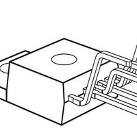
IC OFFLINE CTLR SMPS OTP TO220-6
Manufacturer
Infineon Technologies
Series
CoolSET®F3Rr
Type
Off Line Switcherr
Specifications of ICE3BR0665JF
Output Isolation
Isolated
Frequency Range
58 ~ 75kHz
Voltage - Input
10.5 ~ 27 V
Voltage - Output
650V
Power (watts)
42W
Operating Temperature
-25°C ~ 130°C
Package / Case
TO-220-6 Formed Leads
Output Voltage
650 V
Input / Supply Voltage (max)
27 V
Input / Supply Voltage (min)
- 0.3 V
Duty Cycle (max)
75 %
Switching Frequency
67 KHz
Operating Temperature Range
- 25 C to + 130 C
Mounting Style
Through Hole
Maximum Operating Temperature
+ 130 C
Minimum Operating Temperature
- 25 C
Output Power
259 W
Lead Free Status / RoHS Status
Lead free / RoHS Compliant
Other names
SP000366360
Available stocks
Company
Part Number
Manufacturer
Quantity
Price
Company:
Part Number:
ICE3BR0665JF
Manufacturer:
INFINEON
Quantity:
3 400
3.5.3
Figure 15
The driver-stage is optimized to minimize EMI and to
provide high circuit efficiency. This is done by reducing
the switch on slope when exceeding the internal
CoolMOS
control of the rising edge at the driver’s output (see
Figure 9).
Figure 16
Thus the leading switch on spike is minimized.
Furthermore the driver circuit is designed to eliminate
cross conduction of the output stage.
During power up, when VCC is below the undervoltage
lockout threshold V
is set to low in order to disable power transfer to the
secondary side.
Version 2.0
(internal)
V
PWM-Latch
Gate Driver
Gate
5V
®
Gate Driver
VCC
threshold. This is achieved by a slope
1
Gate Driver
Gate Rising Slope
VCCoff
, the output of the Gate Driver
ca. t = 130ns
Gate
CoolMOS
t
®
13
3.6
Figure 17
There is a cycle by cycle peak current limiting operation
realized by the Current-Limit comparator C10. The
source current of the integrated CoolMOS
via an external sense resistor R
R
voltage V
V
comparator C10 immediately turns off the gate drive by
resetting the PWM Latch FF1.
A Propagation Delay Compensation is added to
support the immediate shut down of the integrated
CoolMOS
influence of the AC input voltage on the maximum
output power can be reduced to minimal.
In order to prevent the current limit from distortions
caused by leading edge spikes, a Leading Edge
Blanking is integrated in the current sense path for the
comparators C10, C12 and the PWM-OP.
The output of comparator C12 is activated by the Gate
G10 if Active Burst Mode is entered. When it is
activated, the current limiting is reduced to 0.26V. This
voltage level determines the maximum power level in
Active Burst Mode.
PWM Latch
Sense
Sense
FF1
PWM-OP
Active Burst
exceeds the internal threshold voltage V
the source current is transformed to a sense
Mode
Sense
®
G10
with very short propagation delay. Thus the
Current Limiting
&
Propagation-Delay
Current Limiting Block
which is fed into the pin CS. If the voltage
Compensation
CS
C10
C12
Functional Description
10k
ICE3BR0665JF
CoolSET
0.26V
V
D1
csth
Sense
Current Limiting
. By means of
Blanking
Leading
11 Sep 2008
220ns
Edge
1pF
®
is sensed
®
-F3R
csth,
the


