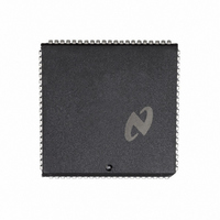
DP8422AV-25 National Semiconductor, DP8422AV-25 Datasheet - Page 6

DP8422AV-25
Manufacturer Part Number
DP8422AV-25
Description
IC CTRLR/DVR CMOS PROGRAM 84PLCC
Manufacturer
National Semiconductor
Datasheet
1.DP8420AV-25.pdf
(58 pages)
Specifications of DP8422AV-25
Controller Type
Dynamic RAM (DRAM)
Voltage - Supply
4.5 V ~ 5.5 V
Operating Temperature
0°C ~ 70°C
Package / Case
84-PLCC
Lead Free Status / RoHS Status
Contains lead / RoHS non-compliant
Other names
*DP8422AV-25
Available stocks
Company
Part Number
Manufacturer
Quantity
Price
Company:
Part Number:
DP8422AV-25
Manufacturer:
NDK
Quantity:
3
Company:
Part Number:
DP8422AV-25
Manufacturer:
Texas Instruments
Quantity:
10 000
Part Number:
DP8422AV-25
Manufacturer:
NS/国半
Quantity:
20 000
2 3 REFRESH SIGNALS
2 4 PORT A ACCESS SIGNALS
RFIP
RFSH
DISRFSH
ADS
(ALE)
CS
AREQ
WAIT
(DTACK)
WAITIN
2 0 Signal Descriptions
Name
Pin
Applicable to All)
Device (If not
Output
Input
O
O
O
I
I
I
I
I
I
I
(Continued)
REFRESH IN PROGRESS This output is asserted prior to a refresh cycle and is
negated when all the RAS outputs are negated for that refresh
REFRESH This input asserted with DISRFRSH already asserted will request a
refresh If this input is continually asserted the DP8420A 21A 22A will perform
refresh cycles in a burst refresh fashion until the input is negated If RFSH is asserted
with DISRFSH negated the internal refresh address counter is cleared (useful for
burst refreshes)
DISABLE REFRESH This input is used to disable internal refreshes and must be
asserted when using RFSH for externally requested refreshes
ADDRESS STROBE or ADDRESS LATCH ENABLE Depending on programming
this input can function as ADS or ALE In mode 0 the input functions as ALE and
when asserted along with CS causes an internal latch to be set Once this latch is set
an access will start from the positive clock edge of CLK as soon as possible In Mode
1 the input functions as ADS and when asserted along with CS causes the access
RAS to assert if no other event is taking place If an event is taking place RAS will be
asserted from the positive edge of CLK as soon as possible In both cases the low
going edge of this signal latches the bank row and column address if programmed to
do so
CHIP SELECT This input signal must be asserted to enable a Port A access
ACCESS REQUEST This input signal in Mode 0 must be asserted some time after
the first positive clock edge after ALE has been asserted When this signal is
negated RAS is negated for the access In Mode 1 this signal must be asserted
before ADS can be negated When this signal is negated RAS is negated for the
access
WAIT or DTACK This output can be programmed to insert wait states into a CPU
access cycle With R7 negated during programming the output will function as a
WAIT type output In this case the output will be active low to signal a wait condition
With R7 asserted during programming the output will function as DTACK In this
case the output will be negated to signify a wait condition and will be asserted to
signify the access has taken place Each of these signals can be delayed by a
number of positive clock edges or negative clock levels of CLK to increase the
microprocessor’s access cycle through the insertion of wait states
WAIT INCREASE This input can be used to dynamically increase the number of
positive clock edges of CLK until DTACK will be asserted or WAIT will be negated
during a DRAM access
6
Description


