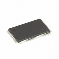
MCM69C432TQ20 Freescale Semiconductor, MCM69C432TQ20 Datasheet - Page 11

MCM69C432TQ20
Manufacturer Part Number
MCM69C432TQ20
Description
IC CAM 1MB 50MHZ 100LQFP
Manufacturer
Freescale Semiconductor
Datasheet
1.MCM69C432TQ20.pdf
(20 pages)
Specifications of MCM69C432TQ20
Format - Memory
RAM
Memory Type
CAM
Memory Size
1M (16K x 64)
Speed
50MHz
Interface
Parallel
Voltage - Supply
3.135 V ~ 3.465 V
Operating Temperature
0°C ~ 70°C
Package / Case
100-LQFP
Lead Free Status / RoHS Status
Contains lead / RoHS non-compliant
Available stocks
Company
Part Number
Manufacturer
Quantity
Price
Company:
Part Number:
MCM69C432TQ20
Manufacturer:
Freescale Semiconductor
Quantity:
10 000
MOTOROLA FAST SRAM
shortest–lived entries are placed near the end of the table.
For an ATM application, this would correspond to the assign-
ment of small VPI values to permanent virtual circuits and
large VPI values to switched virtual circuits.
CAM via the fast–entry mode, the process is dominated by
the time it takes to execute the initialization instruction that
follows. The resulting effective rate of loading the CAM at
start–up is approximately 240,000 entries per second.
RESET
and entry queue. The flag register is set to 1C 16 (setting the
queue empty, buffered–entry mode, and table initialized bits).
The error register is set to FFFF 16 , indicating no errors.
Finally, the almost–full register is set to 3FFF 16 .
CONTROL PORT
Data transfers, both read and write, are initiated by the
assertion of the SEL signal. Address values should be valid
and WE should be high, when SEL is asserted to begin
a read cycle. All values (address, WE, and SEL) should be
held until the MCM69C432 asserts DTACK to signal the end
of the read cycle.
be low, when SEL is asserted to begin a write cycle. Address,
data, WE, and SEL values should be held until the
MCM69C432 asserts DTACK to signal the end of the write
cycle.
MATCH PORT
tion. When the match width is
initiated by presenting the match data on MQ31 – MQ0 and
Note that at start–up, when entries are loaded into the
Asserting RESET removes all entries from the CAM table
The control port of the MCM69C432 is asynchronous.
Address and data values should be valid and WE should
The MCM69C432’s match port is synchronous in opera-
TIMING OVERVIEW
2,500
2,000
1,500
1,000
500
0
220
v
32 bits, a match cycle can be
Figure 3. Connections per Second vs Match Cycle Time
Freescale Semiconductor, Inc.
320
For More Information On This Product,
Go to: www.freescale.com
420
MATCH DUTY CYCLE AT 50 MHz INPUT CLOCK
520
asserting the LH/SM signal with the appropriate setup time
relative to the rising edge of the clock. The assertion of the
MC output signifies the completion of the match cycle. If a
match has been found, the MS output is also asserted. If the
match is a virtual path circuit match in ATM mode, the VPC
output will be asserted with the MS output. Output data, if
any, is enabled by the assertion of the G input.
first latched into the MCM69C432 by the LL input. The match
cycle is then initiated as specified in the previous paragraph.
SIMULTANEOUS PORT OPERATIONS
neously, certain procedures must be followed. If a CHECK
FOR VALUE command is issued, both the last operation
complete bit (bit 10) and the entry queue empty bit (bit 4) in
the flag register should be set prior to executing the CHECK
FOR VALUE command in order to receive valid results. How-
ever, matching on the match port can be done directly after
the last operation complete flag is set.
simultaneous operations.
DEPTH EXPANSION
the match table. The hardware requirements are very
straightforward, as the following pins on each device are sim-
ply wired in parallel: A2 – A0, DQ15 – DQ0, WE, IRQ,
DTACK, MQ31 – MQ0, K, G, LH/SM, MC, MS, and VPC.
Four CAMs can be easily cascaded. Simulations show that
eight devices can be cascaded if care is taken to minimize
the length of the PC board traces connecting the CAMs.
entries in a single CAM. The check for value instruction
should be used to verify that multiple matching entries will
not result from a potential new entry. If a match is found in
CAM 1, for example, the new value should be placed in CAM 1,
where it will replace the existing entry.
620
If the match width is greater than 32 bits, the lower bits are
When the control and match ports are utilized simulta-
The match port has priority over the control port during
Multiple CAMs can be cascaded to increase the depth of
The buffered–entry mode prevents multiple matching
720
820
TYPICAL
WORST CASE
MCM69C432 SCM69C432
920
1020
11


