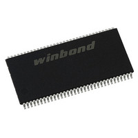
W9412G6IH-5 Winbond Electronics, W9412G6IH-5 Datasheet - Page 25

W9412G6IH-5
Manufacturer Part Number
W9412G6IH-5
Description
IC DDR-400 SDRAM 128MB 66TSSOPII
Manufacturer
Winbond Electronics
Datasheet
1.W9412G6IH-5.pdf
(53 pages)
Specifications of W9412G6IH-5
Format - Memory
RAM
Memory Type
DDR SDRAM
Memory Size
128M (8Mx16)
Speed
250MHz
Interface
Parallel
Voltage - Supply
2.3 V ~ 2.7 V
Operating Temperature
0°C ~ 70°C
Package / Case
66-TSOPII
Lead Free Status / RoHS Status
Lead free / RoHS Compliant
Available stocks
Company
Part Number
Manufacturer
Quantity
Price
Part Number:
W9412G6IH-5
Manufacturer:
WINBOND/华邦
Quantity:
20 000
9.5
SYM.
I
I
I
I
I
I
DD4W
I
I
DD2P
DD2N
DD3P
DD3N
DD4R
I
I
I
DD0
DD1
DD5
DD6
DD7
DC Characteristics
Operating current: One Bank Active-Precharge;
t
DQ, DM and DQS inputs changing once per clock cycle;
Address and control inputs changing once every two clock cycles.
Operating current: One Bank Active-Read-Precharge;
Burst = 4; t
Address and control inputs changing once per clock cycle
Precharge Power Down standby current:
All Banks Idle; Power down mode;
CKE < V
Idle standby current:
Address and other control inputs changing once per clock cycle;
Vin > V
Active Power Down standby current:
One Bank Active; Power down mode;
CKE < V
Vin = V
Active standby current:
t
DQ, DM and DQS inputs changing twice per clock cycle;
Address and other control inputs changing once per clock cycle
Operating current:
Burst = 2; Reads; Continuous burst; One Bank Active;
Address and control inputs changing once per clock cycle;
CL=2; t
Operating current:
Burst = 2; Write; Continuous burst; One Bank Active;
Address and control inputs changing once per clock cycle;
CL = 2; t
DQ, DM and DQS inputs changing twice per clock cycle.
Auto Refresh current: t
Self Refresh current: CKE < 0.2V; external clock on; t
Random Read current: 4 Banks Active Read with activate every
20nS, Auto-Precharge Read every 20 nS;
Burst = 4; t
DQ, DM and DQS inputs changing twice per clock cycle;
Address changing once per clock cycle.
CS > V
CS > V
RC
RC
= t
= t
RC
RAS
IH
REF
CK
CK
IL
IL
IH
IH
min; t
min or Vin < V
= t
max; t
max; t
max; t
RC
RCD
min; All Banks Idle; CKE > V
min; CKE > V
for DQ, DQS and DM
= t
CK
= t
CK
CK
= 3; I
min; I
CK
RC
CK
CK
min;
= t
= t
min; CL = 3; t
= t
= t
OUT
CK
OUT
CK
CK
CK
RC
min;
IL
= 0mA;
PARAMETER
IH
min;
min; Vin = V
min;
= 0mA.
= t
max for DQ, DQS and DM
min; One Bank Active-Precharge;
RFC
min.
.
CK
= t
REF
CK
IH
min; I
for DQ, DQS and DM
min; t
OUT
CK
= t
- 25 -
= 0 mA;
.
CK
CK
min;
= t
.
CK
min.
.
.
-4
130
140
185
185
200
320
Publication Release Date: Sep. 16, 2009
20
45
20
60
3
MAX.
-5/-5I
130
140
180
180
200
320
20
45
20
60
3
-6/-6I
W9412G6IH
120
130
170
170
190
300
20
45
20
60
3
UNIT
mA
Revision A06
NOTES
7, 9
7, 9
7
7
7
7
7


