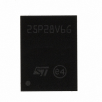
M25P128-VME6G NUMONYX, M25P128-VME6G Datasheet - Page 31

M25P128-VME6G
Manufacturer Part Number
M25P128-VME6G
Description
IC FLASH 128MBIT 50MHZ 8VDFPN
Manufacturer
NUMONYX
Series
Forté™r
Datasheet
1.M25P128-VME6TGB.pdf
(47 pages)
Specifications of M25P128-VME6G
Format - Memory
FLASH
Memory Type
FLASH
Memory Size
128M (16M x 8)
Speed
50MHz
Interface
SPI, 3-Wire Serial
Voltage - Supply
2.7 V ~ 3.6 V
Operating Temperature
-40°C ~ 85°C
Package / Case
8-VDFPN
Cell Type
NOR
Density
128Mb
Access Time (max)
8ns
Interface Type
Serial (SPI)
Boot Type
Not Required
Address Bus
1b
Operating Supply Voltage (typ)
3.3V
Operating Temp Range
-40C to 85C
Package Type
VDFPN EP
Sync/async
Synchronous
Operating Temperature Classification
Industrial
Operating Supply Voltage (min)
2.7V
Operating Supply Voltage (max)
3.6V
Word Size
8b
Number Of Words
16M
Supply Current
8mA
Mounting
Surface Mount
Pin Count
8
Lead Free Status / RoHS Status
Lead free / RoHS Compliant
Available stocks
Company
Part Number
Manufacturer
Quantity
Price
Part Number:
M25P128-VME6G
Manufacturer:
MICRON/镁光
Quantity:
20 000
Company:
Part Number:
M25P128-VME6GB
Manufacturer:
NUMONYX
Quantity:
1 920
Company:
Part Number:
M25P128-VME6GB
Manufacturer:
SILICON
Quantity:
2 310
Part Number:
M25P128-VME6GB
Manufacturer:
ST
Quantity:
20 000
6.10
Bulk erase (BE)
The Bulk Erase (BE) instruction sets all bits to 1 (FFh). Before it can be accepted, a Write
Enable (WREN) instruction must previously have been executed. After the Write Enable
(WREN) instruction has been decoded, the device sets the Write Enable Latch (WEL).
The Bulk Erase (BE) instruction is entered by driving Chip Select (S) Low, followed by the
instruction code on Serial Data Input (D). Chip Select (S) must be driven Low for the entire
duration of the sequence.
The instruction sequence is shown in
Chip Select (S) must be driven High after the eighth bit of the instruction code has been
latched in, otherwise the Bulk Erase instruction is not executed. As soon as Chip Select (S)
is driven High, the self-timed Bulk Erase cycle (whose duration is t
Bulk Erase cycle is in progress, the Status Register may be read to check the value of the
Write In Progress (WIP) bit. The Write In Progress (WIP) bit is 1 during the self-timed Bulk
Erase cycle, and is 0 when it is completed. At some unspecified time before the cycle is
completed, the Write Enable Latch (WEL) bit is reset.
The Bulk Erase (BE) instruction is executed only if all Block Protect (BP2, BP1, BP0) bits
are 0. The Bulk Erase (BE) instruction is ignored if one, or more, sectors are protected.
Figure 17. Bulk erase (BE) instruction sequence
S
C
D
0
Figure
1
2
Instruction
17.
3
4
5
6
7
AI03752D
BE
) is initiated. While the
31/47


