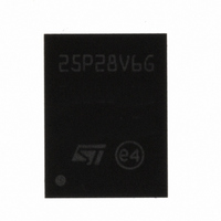
M25P128-VME6G NUMONYX, M25P128-VME6G Datasheet - Page 19

M25P128-VME6G
Manufacturer Part Number
M25P128-VME6G
Description
IC FLASH 128MBIT 50MHZ 8VDFPN
Manufacturer
NUMONYX
Series
Forté™r
Datasheet
1.M25P128-VME6TGB.pdf
(47 pages)
Specifications of M25P128-VME6G
Format - Memory
FLASH
Memory Type
FLASH
Memory Size
128M (16M x 8)
Speed
50MHz
Interface
SPI, 3-Wire Serial
Voltage - Supply
2.7 V ~ 3.6 V
Operating Temperature
-40°C ~ 85°C
Package / Case
8-VDFPN
Cell Type
NOR
Density
128Mb
Access Time (max)
8ns
Interface Type
Serial (SPI)
Boot Type
Not Required
Address Bus
1b
Operating Supply Voltage (typ)
3.3V
Operating Temp Range
-40C to 85C
Package Type
VDFPN EP
Sync/async
Synchronous
Operating Temperature Classification
Industrial
Operating Supply Voltage (min)
2.7V
Operating Supply Voltage (max)
3.6V
Word Size
8b
Number Of Words
16M
Supply Current
8mA
Mounting
Surface Mount
Pin Count
8
Lead Free Status / RoHS Status
Lead free / RoHS Compliant
Available stocks
Company
Part Number
Manufacturer
Quantity
Price
Part Number:
M25P128-VME6G
Manufacturer:
MICRON/镁光
Quantity:
20 000
Company:
Part Number:
M25P128-VME6GB
Manufacturer:
NUMONYX
Quantity:
1 920
Company:
Part Number:
M25P128-VME6GB
Manufacturer:
SILICON
Quantity:
2 310
Part Number:
M25P128-VME6GB
Manufacturer:
ST
Quantity:
20 000
6
Instructions
All instructions, addresses and data are shifted in and out of the device, most significant bit
first.
Serial Data Input (D) is sampled on the first rising edge of Serial Clock (C) after Chip Select
(S) is driven Low. Then, the one-byte instruction code must be shifted in to the device, most
significant bit first, on Serial Data Input (D), each bit being latched on the rising edges of
Serial Clock (C).
The instruction set is listed in
Every instruction sequence starts with a one-byte instruction code. Depending on the
instruction, this might be followed by address bytes, or by data bytes, or by both or none.
In the case of a Read Data Bytes (READ), Read Data Bytes at Higher Speed (Fast_Read),
Read Status Register (RDSR) or Read Identification (RDID) instruction, the shifted-in
instruction sequence is followed by a data-out sequence. Chip Select (S) can be driven High
after any bit of the data-out sequence is being shifted out.
In the case of a Page Program (PP), Sector Erase (SE), Bulk Erase (BE), Write Status
Register (WRSR), Write Enable (WREN) or Write Disable (WRDI), Chip Select (S) must be
driven High exactly at a byte boundary, otherwise the instruction is rejected, and is not
executed. That is, Chip Select (S) must driven High when the number of clock pulses after
Chip Select (S) being driven Low is an exact multiple of eight.
All attempts to access the memory array during a Write Status Register cycle, Program
cycle or Erase cycle are ignored, and the internal Write Status Register cycle, Program
cycle or Erase cycle continues unaffected.
Table 4.
FAST_READ
Instruction
WREN
WRSR
RDSR
READ
WRDI
RDID
PP
SE
BE
Instruction set
Read Identification
Read Status Register
Read Data Bytes
Page Program
Sector Erase
Bulk Erase
Write Enable
Write Disable
Write Status Register
Read Data Bytes at Higher
Speed
Description
Table
4.
One-byte Instruction
0000 0100
0000 0101
0000 0001
0000 0010
0000 0110
0000 0011
0000 1011
1101 1000
1001 1111
1100 0111
Code
9Fh
0Bh
D8h
C7h
06h
04h
05h
01h
03h
02h
Address
Bytes
0
0
0
0
0
3
3
3
3
0
Dummy
Bytes
0
0
0
0
0
0
1
0
0
0
1 to 256
Bytes
1 to ∞
1 to ∞
1 to ∞
1 to 3
Data
0
0
1
0
0
19/47


