M25P128-VME6G NUMONYX, M25P128-VME6G Datasheet - Page 13
M25P128-VME6G
Manufacturer Part Number
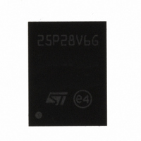
M25P128-VME6G
Description
IC FLASH 128MBIT 50MHZ 8VDFPN
Manufacturer
NUMONYX
Series
Forté™r
Datasheet
1.M25P128-VME6TGB.pdf
(47 pages)
Specifications of M25P128-VME6G
Format - Memory
FLASH
Memory Type
FLASH
Memory Size
128M (16M x 8)
Speed
50MHz
Interface
SPI, 3-Wire Serial
Voltage - Supply
2.7 V ~ 3.6 V
Operating Temperature
-40°C ~ 85°C
Package / Case
8-VDFPN
Cell Type
NOR
Density
128Mb
Access Time (max)
8ns
Interface Type
Serial (SPI)
Boot Type
Not Required
Address Bus
1b
Operating Supply Voltage (typ)
3.3V
Operating Temp Range
-40C to 85C
Package Type
VDFPN EP
Sync/async
Synchronous
Operating Temperature Classification
Industrial
Operating Supply Voltage (min)
2.7V
Operating Supply Voltage (max)
3.6V
Word Size
8b
Number Of Words
16M
Supply Current
8mA
Mounting
Surface Mount
Pin Count
8
Lead Free Status / RoHS Status
Lead free / RoHS Compliant
Available stocks
Company
Part Number
Manufacturer
Quantity
Price

Part Number:
M25P128-VME6G
Manufacturer:
MICRON/镁光
Quantity:
20 000
Company:
Part Number:
M25P128-VME6GB
Manufacturer:
NUMONYX
Quantity:
1 920
Company:
Part Number:
M25P128-VME6GB
Manufacturer:
SILICON
Quantity:
2 310
Part Number:
M25P128-VME6GB
Manufacturer:
ST
Quantity:
20 000


4.5
4.6
4.7
Active power and standby power modes
When Chip Select (S) is Low, the device is selected, and in the Active Power mode.
When Chip Select (S) is High, the device is deselected, but could remain in the Active
Power mode until all internal cycles have completed (Program, Erase, Write Status
Register). The device then goes in to the Standby Power mode. The device consumption
drops to I
Status register
The Status Register contains a number of status and control bits that can be read or set (as
appropriate) by specific instructions. See
detailed description of the Status Register bits.
Protection modes
The environments where non-volatile memory devices are used can be very noisy. No SPI
device can operate correctly in the presence of excessive noise. To help combat this, the
M25P128 features the following data protection mechanisms:
Power On Reset and an internal timer (t
inadvertent changes while the power supply is outside the operating specification.
Program, Erase and Write Status Register instructions are checked that they consist of
a number of clock pulses that is a multiple of eight, before they are accepted for
execution.
All instructions that modify data must be preceded by a Write Enable (WREN)
instruction to set the Write Enable Latch (WEL) bit. This bit is returned to its reset state
by the following events:
–
–
–
–
–
–
The Block Protect (BP2, BP1, BP0) bits allow part of the memory to be configured as
read-only. This is the Software Protected Mode (SPM).
The Write Protect (W/V
Status Register Write Disable (SRWD) bit to be protected. This is the Hardware
Protected Mode (HPM).
CC1
Power-up
Write Disable (WRDI) instruction completion
Write Status Register (WRSR) instruction completion
Page Program (PP) instruction completion
Sector Erase (SE) instruction completion
Bulk Erase (BE) instruction completion
.
PP
) signal allows the Block Protect (BP2, BP1, BP0) bits and
Section 6.4: Read status register (RDSR)
PUW
) can provide protection against
for a
13/47
Related parts for M25P128-VME6G
Image
Part Number
Description
Manufacturer
Datasheet
Request
R

Part Number:
Description:
IC FLASH 128MBIT 50MHZ 16SOIC
Manufacturer:
NUMONYX
Datasheet:

Part Number:
Description:
IC FLASH 128MBIT 65NM 3V 8VDFPN
Manufacturer:
NUMONYX
Datasheet:
Part Number:
Description:
IC FLASH 128MBIT 65NM 3V SO16
Manufacturer:
NUMONYX
Datasheet:

Part Number:
Description:
IC FLASH 128MBIT 50MHZ 16SOIC
Manufacturer:
NUMONYX
Datasheet:
Part Number:
Description:
FLASH SERL-SPI 3.3V 128MBIT 16MX8 8NS 16SOIC W
Manufacturer:
NUMONYX
Part Number:
Description:
FLASH SERL-SPI 3.3V 128MBIT 16MX8 8NS 8PIN VDFPN
Manufacturer:
NUMONYX
Part Number:
Description:
IC FLASH 128MBIT 50MHZ 8VDFPN
Manufacturer:
NUMONYX
Datasheet:

Part Number:
Description:
128 Mbit (Multilevel), low-voltage, Serial Flash memory with 50-MHz SPI bus interface
Manufacturer:
Numonyx, B.V.
Datasheet:
Part Number:
Description:
128 Mbit (Multilevel), low-voltage, Serial Flash memory with 50-MHz SPI bus interface
Manufacturer:
Numonyx, B.V.
Datasheet:
Part Number:
Description:
Numonyx� Embedded Flash Memory J3 V. D
Manufacturer:
Numonyx
Datasheet: