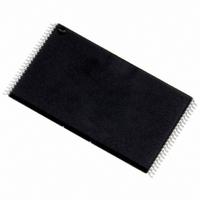
NAND256W3A2BN6F STMicroelectronics, NAND256W3A2BN6F Datasheet - Page 28

NAND256W3A2BN6F
Manufacturer Part Number
NAND256W3A2BN6F
Description
IC FLASH 256MBIT 48TSOP
Manufacturer
STMicroelectronics
Datasheet
1.NAND128W3A2BN6E.pdf
(59 pages)
Specifications of NAND256W3A2BN6F
Format - Memory
FLASH
Memory Type
FLASH - Nand
Memory Size
256M (32M x 8)
Interface
Parallel
Voltage - Supply
2.7 V ~ 3.6 V
Operating Temperature
-40°C ~ 85°C
Package / Case
48-TSOP
Lead Free Status / RoHS Status
Lead free / RoHS Compliant
Speed
-
Available stocks
Company
Part Number
Manufacturer
Quantity
Price
Company:
Part Number:
NAND256W3A2BN6F
Manufacturer:
ST
Quantity:
4 000
Part Number:
NAND256W3A2BN6F
Manufacturer:
ST
Quantity:
20 000
Device operations
6.4
28/59
Copy back program
The copy back program operation copies the data stored in one page and reprogram it in
another page.
The copy back program operation does not require external memory and so the operation is
faster and more efficient because the reading and loading cycles are not required. The
operation is particularly useful when a portion of a block is updated and the rest of the block
needs to be copied to the newly assigned block.
If the copy back program operation fails an error is signalled in the status register. However,
as the standard external ECC cannot be used with the copy back operation bit error due to
charge loss cannot be detected. For this reason it is recommended to limit the number of
copy back operations on the same data and or to improve the performance of the ECC.
The copy back program operation requires the following three steps:
1.
2.
3.
After a copy back program operation, a partial-page program is not allowed in the target
page until the block has been erased. See
operation.
Table 10.
Figure 15. Copy back operation
RB
I/O
The source page must be read using the Read A command (one bus write cycle to
setup the command and then 4 bus write cycles to input the source page address).
This operation copies all 264 words/ 528 bytes from the page into the page buffer.
When the device returns to the ready state (Ready/Busy High), the second bus write
cycle of the command is given with the 4 bus cycles to input the target page address.
Refer to
pages.
Then the confirm command is issued to start the P/E/R controller.
Read
Code
00h
128 Mbits
256 Mbits
Density
Copy back program addresses
Table 10
Address Inputs
Source
(Read Busy time)
for the addresses that must be the same for the source and target
tBLBH1
Copy Back
8Ah
Code
Same address for source and target pages
Figure 15
Address Inputs
Target
for an example of the copy back
(Program Busy time)
tBLBH2
A23
A24
10h
NAND128-A, NAND256-A
Busy
Read Status Register
70h
SR0
ai07590b


