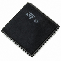
PSD834F2-90JI STMicroelectronics, PSD834F2-90JI Datasheet - Page 67

PSD834F2-90JI
Manufacturer Part Number
PSD834F2-90JI
Description
IC FLASH 2MBIT 90NS 52PLCC
Manufacturer
STMicroelectronics
Datasheet
1.PSD813F2VA-20JI.pdf
(109 pages)
Specifications of PSD834F2-90JI
Format - Memory
FLASH
Memory Type
FLASH
Memory Size
2M (256K x 8)
Speed
90ns
Interface
Parallel
Voltage - Supply
4.5 V ~ 5.5 V
Operating Temperature
-40°C ~ 85°C
Package / Case
52-PLCC
Lead Free Status / RoHS Status
Contains lead / RoHS non-compliant
Other names
497-2007-5
Available stocks
Company
Part Number
Manufacturer
Quantity
Price
Company:
Part Number:
PSD834F2-90JI
Manufacturer:
SANYO
Quantity:
120
Company:
Part Number:
PSD834F2-90JI
Manufacturer:
STMicroelectronics
Quantity:
10 000
Part Number:
PSD834F2-90JI
Manufacturer:
WSI
Quantity:
20 000
RESET TIMING AND DEVICE STATUS AT RESET
Power-Up Reset
Upon Power-up, the PSD requires a Reset (RE-
SET) pulse of duration t
steady. During this period, the device loads inter-
nal configurations, clears some of the registers
and sets the Flash memory into Operating mode.
After the rising edge of Reset (RESET), the PSD
remains in the Reset mode for an additional peri-
od, t
lowed.
The Flash memory is reset to the READ Mode
upon Power-up. Sector Select (FS0-FS7 and
CSBOOT0-CSBOOT3) must all be Low, Write
Strobe (WR, CNTL0) High, during Power On Re-
set for maximum security of the data contents and
to remove the possibility of a byte being written on
the first edge of Write Strobe (WR, CNTL0). Any
Flash memory WRITE cycle initiation is prevented
automatically when V
Warm Reset
Once the device is up and running, the device can
be reset with a pulse of a much shorter duration,
t
Figure 34. Reset (RESET) Timing
NLNH
V
RESET
OPR
.
CC
, before the first memory access is al-
CC
Power-On Reset
V
is below V
t NLNH-PO
CC
(min)
NLNH-PO
LKO
after V
.
Doc ID 10552 Rev 3
t OPR
CC
is
The same t
is operational after warm reset. Figure
the timing of the Power-up and warm reset.
I/O Pin, Register and PLD Status at Reset
Table 33., page 68
PLD status during Power On Reset, warm reset
and Power-down mode. PLD outputs are always
valid during warm reset, and they are valid in Pow-
er On Reset once the internal PSD Configuration
bits are loaded. This loading of PSD is completed
typically long before the V
ing level. Once the PLD is active, the state of the
outputs are determined by the PSDabel equa-
tions.
Reset of Flash Memory Erase and Program
Cycles (on the PSD834Fx)
A Reset (RESET) also resets the internal Flash
memory state machine. During a Flash memory
Program or Erase cycle, Reset (RESET) termi-
nates the cycle and returns the Flash memory to
the Read Mode within a period of t
OPR
period is needed before the device
shows the I/O pin, register and
Warm Reset
PSD813F2V, PSD854F2V
t NLNH-A
t NLNH
CC
ramps up to operat-
NLNH-A
t OPR
AI02866b
34
.
shows
67/109


