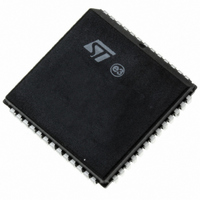
PSD834F2-90JI STMicroelectronics, PSD834F2-90JI Datasheet - Page 56

PSD834F2-90JI
Manufacturer Part Number
PSD834F2-90JI
Description
IC FLASH 2MBIT 90NS 52PLCC
Manufacturer
STMicroelectronics
Datasheet
1.PSD813F2VA-20JI.pdf
(109 pages)
Specifications of PSD834F2-90JI
Format - Memory
FLASH
Memory Type
FLASH
Memory Size
2M (256K x 8)
Speed
90ns
Interface
Parallel
Voltage - Supply
4.5 V ~ 5.5 V
Operating Temperature
-40°C ~ 85°C
Package / Case
52-PLCC
Lead Free Status / RoHS Status
Contains lead / RoHS non-compliant
Other names
497-2007-5
Available stocks
Company
Part Number
Manufacturer
Quantity
Price
Company:
Part Number:
PSD834F2-90JI
Manufacturer:
SANYO
Quantity:
120
Company:
Part Number:
PSD834F2-90JI
Manufacturer:
STMicroelectronics
Quantity:
10 000
Part Number:
PSD834F2-90JI
Manufacturer:
WSI
Quantity:
20 000
PSD813F2V, PSD854F2V
JTAG In-System Programming (ISP)
Port C is JTAG compliant, and can be used for In-
System Programming (ISP). You can multiplex
JTAG operations with other functions on Port C
because In-System Programming (ISP) is not per-
formed in normal Operating mode. For more infor-
mation on the JTAG Port, see the section entitled
PROGRAMMING IN-CIRCUIT USING THE JTAG
SERIAL INTERFACE, page
Port Configuration Registers (PCR)
Each Port has a set of Port Configuration Regis-
ters (PCR) used for configuration. The contents of
the registers can be accessed by the MCU through
normal READ/WRITE bus cycles at the addresses
given in
ble
of the CSIOP register.
The pins of a port are individually configurable and
each bit in the register controls its respective pin.
For example, Bit 0 in a register refers to Bit 0 of its
port. The three Port Configuration Registers
(PCR), shown in Table 22, are used for setting the
Port configurations. The default Power-up state for
each register in Table
Control Register
Any bit reset to '0' in the Control Register sets the
corresponding port pin to MCU I/O Mode, and a '1'
sets it to Address Out Mode. The default mode is
MCU I/O. Only Ports A and B have an associated
Control Register.
Direction Register
The Direction Register, in conjunction with the out-
put enable (except for Port D), controls the direc-
tion of data flow in the I/O Ports. Any bit set to '1'
in the Direction Register causes the correspond-
ing pin to be an output, and any bit set to '0' causes
it to be an input. The default mode for all port pins
is input.
Figure 28., page 58
the Port Architecture diagrams for Ports A/B and
C, respectively. The direction of data flow for Ports
A, B, and C are controlled not only by the direction
register, but also by the output enable product
term from the PLD AND Array. If the output enable
product term is not active, the Direction Register
has sole control of a given pin’s direction.
An example of a configuration for a Port with the
three least significant bits set to output and the re-
mainder set to input is shown in Table 25. Since
Port D only contains three pins (shown in
31., page
has only the three least significant bits active.
56/109
7
are the offsets in hexadecimal from the base
Table 7., page
61), the Direction Register for Port D
and
22
18. The addresses in Ta-
Figure 29., page 59
is 00h.
69.
Doc ID 10552 Rev 3
Figure
show
Note: 1. See
Table 23. Port Pin Direction Control, Output
Enable P.T. Not Defined
Table 24. Port Pin Direction Control, Output
Enable P.T. Defined
Table 25. Port Direction Assignment Example
Drive Select Register
The Drive Select Register configures the pin driver
as Open Drain or CMOS for some port pins, and
controls the slew rate for the other port pins. An
external pull-up resistor should be used for pins
configured as Open Drain.
A pin can be configured as Open Drain if its corre-
sponding bit in the Drive Select Register is set to a
’1.’ The default pin drive is CMOS.
Note that the slew rate is a measurement of the
rise and fall times of an output. A higher slew rate
means a faster output response and may create
more electrical noise. A pin operates in a high slew
rate when the corresponding bit in the Drive Reg-
ister is set to ’1.’ The default rate is slow slew.
Table 26., page 57
Ports A, B, C, and D. It summarizes which pins can
be configured as Open Drain outputs and which
pins the slew rate can be set for.
Table 22. Port Configuration Registers (PCR)
Control
Direction
Drive Select
0
1
0
0
1
1
0
Bit 7
Register Name
Direction Register Bit
Register Bit
Direction
0
Bit 6
Table 26., page 57
1
0
Bit 5
A,B
A,B,C,D
A,B,C,D
0
1
0
1
Output Enable
0
Bit 4
shows the Drive Register for
Port
P.T.
for Drive Register bit definition.
Input
Output
0
Bit 3
Port Pin Mode
1
Bit 2
WRITE/READ
WRITE/READ
WRITE/READ
Input
Output
Output
Output
Port Pin Mode
MCU Access
1
Bit 1
1
Bit 0


