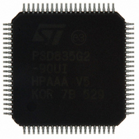
PSD835G2-90UI STMicroelectronics, PSD835G2-90UI Datasheet - Page 80

PSD835G2-90UI
Manufacturer Part Number
PSD835G2-90UI
Description
IC FLASH 4MBIT 90NS 80TQFP
Manufacturer
STMicroelectronics
Datasheet
1.PSD835G2-90U.pdf
(120 pages)
Specifications of PSD835G2-90UI
Format - Memory
FLASH
Memory Type
FLASH
Memory Size
4M (512K x 8)
Speed
90ns
Interface
Parallel
Voltage - Supply
4.5 V ~ 5.5 V
Operating Temperature
-40°C ~ 85°C
Package / Case
80-TQFP, 80-VQFP
Lead Free Status / RoHS Status
Lead free / RoHS Compliant
Other names
497-2016
Available stocks
Company
Part Number
Manufacturer
Quantity
Price
Company:
Part Number:
PSD835G2-90UI
Manufacturer:
ST
Quantity:
201
Company:
Part Number:
PSD835G2-90UI
Manufacturer:
STMicroelectronics
Quantity:
10 000
I/O ports
Figure 26. Peripheral I/O mode
17.9
17.10
17.11
17.12
80/120
JTAG in-system programming (ISP)
Port E is JTAG compliant, and can be used for In-System Programming (ISP). You can
multiplex JTAG operations with other functions on port E because In-System Programming
(ISP) is not performed in normal Operating mode. For more information on the JTAG port,
see
Port configuration registers (PCR)
Each port has a set of port Configuration registers (PCR) used for configuration. The
contents of the registers can be accessed by the MCU through normal READ/WRITE bus
cycles at the addresses given in
hexadecimal from the base of the CSIOP register.
The pins of a port are individually configurable and each bit in the register controls its
respective pin. For example, bit 0 in a register refers to bit 0 of its port. The three port
Configuration registers (PCR), shown in
configurations. The default Power-up state for each register in
Control register
Any bit reset to ’0’ in the Control register sets the corresponding port pin to MCU I/O mode,
and a ’1’ sets it to Address Out mode. The default mode is MCU I/O. Only ports E, F and G
have an associated Control register.
Direction register
The Direction register, in conjunction with the output enable (except for port D), controls the
direction of data flow in the I/O ports. Any bit set to ’1’ in the Direction register causes the
corresponding pin to be an output, and any bit set to ’0’ causes it to be an input. The default
mode for all port pins is input.
Figure 27
respectively. The direction of data flow for ports A, B, C and F are controlled not only by the
Section 20: Programming in-circuit using the JTAG/ISP
and
RD
PSEL0
PSEL1
WR
VM REGISTER BIT 7
Figure 28
show the port Architecture diagrams for ports A/B/C and E/F/G,
PSEL
Table
5. The addresses in
Table
DATA BUS
D0 - D7
17, are used for setting the port
Table 5
interface.
Table 17
PF0 - PF7
are the offsets in
is 00h.
AI02886b
PSD835G2


