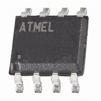
AT26DF081A-SSU Atmel, AT26DF081A-SSU Datasheet - Page 11

AT26DF081A-SSU
Manufacturer Part Number
AT26DF081A-SSU
Description
IC FLASH 8MBIT 70MHZ 8SOIC
Manufacturer
Atmel
Datasheet
1.AT26DF081A-SU.pdf
(40 pages)
Specifications of AT26DF081A-SSU
Format - Memory
FLASH
Memory Type
DataFLASH
Memory Size
8M (4096 pages x 256 bytes)
Speed
70MHz
Interface
SPI, 3-Wire Serial
Voltage - Supply
2.7 V ~ 3.6 V
Operating Temperature
-40°C ~ 85°C
Package / Case
8-SOIC (3.9mm Width)
Lead Free Status / RoHS Status
Lead free / RoHS Compliant
Available stocks
Company
Part Number
Manufacturer
Quantity
Price
Part Number:
AT26DF081A-SSU
Manufacturer:
ATMEL
Quantity:
20 000
Part Number:
AT26DF081A-SSU-B
Manufacturer:
ATMEL/爱特梅尔
Quantity:
20 000
Part Number:
AT26DF081A-SSU-T
Manufacturer:
ATMEL/爱特梅尔
Quantity:
20 000
8.2
3600G–DFLASH–06/09
Sequential Program Mode
The Sequential Program Mode improves throughput over the Byte/Page Program command
when the Byte/Page Program command is used to program single bytes only into consecutive
address locations. For example, some systems may be designed to program only a single byte
of information at a time and cannot utilize a buffered Page Program operation due to design
restrictions. In such a case, the system would normally have to perform multiple Byte Program
operations in order to program data into sequential memory locations. This approach can add
considerable system overhead and SPI bus traffic.
The Sequential Programming Mode helps reduce system overhead and bus traffic by incorporat-
ing an internal address counter that keeps track of the byte location to program, thereby
eliminating the need to supply an address sequence to the device for every byte to program.
When using the Sequential Program mode, all address locations to be programmed must be in
the erased state. Before the Sequential Program mode can first be entered, the Write Enable
command must have been previously issued to the device to set the WEL bit of the Status Reg-
ister to a logical “1” state.
To start the Sequential Program Mode, the CS pin must first be asserted, and either an opcode
of ADh or AFh must be clocked into the device. For the first program cycle, three address bytes
must be clocked in after the opcode to designate the first byte location to program. After the
address bytes have been clocked in, the byte of data to be programmed can be sent to the
device. Deasserting the CS pin will start the internally self-timed program operation, and the byte
of data will be programmed into the memory location specified by A23 - A0.
After the first byte has been successfully programmed, a second byte can be programmed by
simply reasserting the CS pin, clocking in the ADh or AFh opcode, and then clocking in the next
byte of data. When the CS pin is deasserted, the second byte of data will be programmed into
the next sequential memory location. The process would be repeated for any additional bytes.
There is no need to reissue the Write Enable command once the Sequential Program Mode has
been entered.
When the last desired byte has been programmed into the memory array, the Sequential
Program Mode operation can be terminated by reasserting the CS pin and sending the
Write Disable command to the device to reset the WEL bit in the Status Register back to the
logical “0” state.
If more than one byte of data is ever clocked in during each program cycle, then only the last
byte of data sent on the SI pin will be stored in the internal latches. The programming of each
byte is internally self-timed and should take place in a time of t
complete byte of data must be clocked into the device before the CS pin is deasserted, and the
CS pin must be deasserted on even byte boundaries (multiples of eight bits); otherwise, the
device will abort the operation, the byte of data will not be programmed into the memory array,
and the WEL bit in the Status Register will be reset back to the logical “0” state.
If the address initially specified by A23 - A0 points to a memory location within a sector that is in
the protected state, then the Sequential Program Mode command will not be executed, and the
device will return to the idle state once the CS pin has been deasserted. The WEL bit in the Sta-
tus Register will also be reset back to the logical “0” state.
There is no address wrapping when using the Sequential Program Mode. Therefore, when the
last byte (0FFFFFh) of the memory array has been programmed, the device will automatically
exit the Sequential Program mode and reset the WEL bit in the Status Register back to the logi-
cal “0” state. In addition, the Sequential Program mode will not automatically skip over protected
BP
. For each program cycle, a
11


