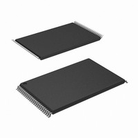
CY62177EV30LL-55ZXI Cypress Semiconductor Corp, CY62177EV30LL-55ZXI Datasheet - Page 5

CY62177EV30LL-55ZXI
Manufacturer Part Number
CY62177EV30LL-55ZXI
Description
IC SRAM 32MBIT 55NS LP 48-TSOP
Manufacturer
Cypress Semiconductor Corp
Datasheet
1.CY62177EV30LL-55ZXI.pdf
(13 pages)
Specifications of CY62177EV30LL-55ZXI
Memory Size
32M (4Mx8, 2Mx16)
Package / Case
48-TSOP I
Format - Memory
RAM
Memory Type
SRAM
Speed
55ns
Interface
Parallel
Voltage - Supply
2.2 V ~ 3.7 V
Operating Temperature
-40°C ~ 85°C
Access Time
55 ns
Supply Voltage (max)
3.7 V
Supply Voltage (min)
2.2 V
Maximum Operating Current
45 mA
Organization
2 M x 16, 4 M x 8
Maximum Operating Temperature
+ 85 C
Minimum Operating Temperature
- 40 C
Mounting Style
SMD/SMT
Operating Supply Voltage
3 V
Lead Free Status / RoHS Status
Lead free / RoHS Compliant
Lead Free Status / RoHS Status
Lead free / RoHS Compliant, Lead free / RoHS Compliant
Available stocks
Company
Part Number
Manufacturer
Quantity
Price
Company:
Part Number:
CY62177EV30LL-55ZXI
Manufacturer:
XILINX
Quantity:
1 000
Part Number:
CY62177EV30LL-55ZXI
Manufacturer:
CYPRESS/赛普拉斯
Quantity:
20 000
Switching Characteristics
Over the Operating Range
Notes
Document #: 001-09880 Rev. *D
Read Cycle
t
t
t
t
t
t
t
t
t
t
t
t
t
t
Write Cycle
t
t
t
t
t
t
t
t
t
t
t
15. Test conditions for all parameters other than tri-state parameters assume signal transition time of 1V/ns, timing reference levels of V
16. At any given temperature and voltage condition, t
17. t
18. The internal Write time of the memory is defined by the overlap of WE, CE
RC
AA
OHA
ACE
DOE
LZOE
HZOE
LZCE
HZCE
PU
PD
DBE
LZBE
HZBE
WC
SCE
AW
HA
SA
PWE
BW
SD
HD
HZWE
LZWE
V
device.
and any of these signals can terminate a write by going INACTIVE. The data input setup and hold timing should be referenced to the edge of the signal that terminates
the write.
HZOE
CC(typ)
Parameter
, t
HZCE
, and output loading of the specified I
, t
[18]
HZBE
, and t
HZWE
[15]
transitions are measured when the outputs enter a high impedence state.
Read Cycle Time
Address to Data Valid
Data Hold from Address Change
CE
OE LOW to Data Valid
OE LOW to LOW Z
OE HIGH to High Z
CE
CE
CE
CE
BLE/BHE LOW to Data Valid
BLE/BHE LOW to Low Z
BLE/BHE HIGH to HIGH Z
Write Cycle Time
CE
Address Setup to Write End
Address Hold from Write End
Address Setup to Write Start
WE Pulse Width
BLE/BHE LOW to Write End
Data Set up to Write End
Data Hold from Write End
WE LOW to High-Z
WE HIGH to Low-Z
1
1
1
1
1
1
LOW and CE
LOW and CE
HIGH and CE
LOW and CE
HIGH and CE
LOW and CE
OL
/I
OH
HZCE
as shown in
2
2
2
2
2
2
[16]
[16, 17]
[16, 17]
[16]
HIGH to Data Valid
HIGH to Low Z
HIGH to Power Up
HIGH to Write End
is less than t
LOW to High Z
LOW to Power Down
Description
[16]
[16, 17]
AC Test Loads
LZCE
, t
[16]
HZBE
1
[16, 17]
= V
IL
is less than t
on page 4.
, BHE and/or BLE = V
LZBE
, t
HZOE
IL
, and CE
is less than t
Min
55
10
10
55
40
40
40
40
25
10
6
5
0
0
0
0
2
= V
CY62177EV30 MoBL
LZOE
IH
. All signals must be ACTIVE to initiate a write
55 ns
, and t
HZWE
CC(typ)
Max
55
55
25
18
18
55
55
18
20
is less than t
/2, input pulse levels of 0 to
LZWE
Page 5 of 13
for any given
Unit
ns
ns
ns
ns
ns
ns
ns
ns
ns
ns
ns
ns
ns
ns
ns
ns
ns
ns
ns
ns
ns
ns
ns
ns
ns
®
[+] Feedback


