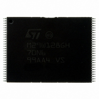
M29W128GH70N6E NUMONYX, M29W128GH70N6E Datasheet - Page 8

M29W128GH70N6E
Manufacturer Part Number
M29W128GH70N6E
Description
IC FLASH 128MBIT 70NS 56TSOP
Manufacturer
NUMONYX
Series
Axcell™r
Datasheet
1.M29W128GH70N6E.pdf
(94 pages)
Specifications of M29W128GH70N6E
Format - Memory
FLASH
Memory Type
FLASH
Memory Size
128M (16Mx8, 8Mx16)
Speed
70ns
Interface
Parallel
Voltage - Supply
2.7 V ~ 3.6 V
Operating Temperature
-40°C ~ 85°C
Package / Case
56-TSOP
Package
56TSOP
Cell Type
NOR
Density
128 Mb
Architecture
Sectored
Block Organization
Symmetrical
Typical Operating Supply Voltage
3|3.3 V
Sector Size
128KByte x 128
Timing Type
Asynchronous
Interface Type
Parallel
Lead Free Status / RoHS Status
Lead free / RoHS Compliant
Available stocks
Company
Part Number
Manufacturer
Quantity
Price
Company:
Part Number:
M29W128GH70N6E
Manufacturer:
Numonyx
Quantity:
17 280
Company:
Part Number:
M29W128GH70N6E
Manufacturer:
MICRON
Quantity:
595
Company:
Part Number:
M29W128GH70N6E
Manufacturer:
MICRON45
Quantity:
556
Part Number:
M29W128GH70N6E
Manufacturer:
ST
Quantity:
20 000
1
8/94
Description
The M29W128GH and M29W128GL are 128-Mbit (8 Mbit x16 or 16 Mbit x8) non-volatile
flash memories that can be read, erased and reprogrammed. These operations can be
performed using a single low voltage (2.7 to 3.6 V) supply. On power-up the memory
defaults to its read mode.
The memory array is divided into 64-Kword/128-Kbyte uniform blocks that can be erased
independently so it is possible to preserve valid data while old data is erased. Program and
Erase commands are written to the command interface of the memory. An on-chip
program/erase controller simplifies the process of programming or erasing the memory by
taking care of all of the special operations that are required to update the memory contents.
The end of a program or erase operation can be detected and any error conditions
identified. The command set required to control the memory is consistent with JEDEC
standards.
Chip Enable, Output Enable and Write Enable signals control the bus operation of the
memory. They allow simple connection to most microprocessors, often without additional
logic.
The M29W128GH and M29W128GL support asynchronous random read and page read
from all blocks of the memory array. The devices also feature a write to buffer program
capability that improves the programming throughput by programming in one shot a buffer of
32 words/64 bytes. The enhanced buffered program feature is also available to speed up
the programming throughput, allowing to program 256 words in one shot (only in x16 mode).
The V
The M29W128GH and M29W128GL have an extra block, the extended block, of 128 words
in x16 mode or of 256 bytes in x8 mode that can be accessed using a dedicated command.
The extended block can be protected and so is useful for storing security information.
However the protection is not reversible, once protected the protection cannot be undone.
The device features different levels of hardware and software block protection to avoid
unwanted program or erase (modify):
The M29W128GH and M29W128GL are offered in TSOP56 (14 x 20 mm), and TBGA64
(10 x 13 mm, 1 mm pitch), packages. The memories are delivered with all the bits erased
(set to ‘1’).
Hardware protection:
–
Software protection:
–
–
–
PP
/WP signal can be used to enable faster programming of the device.
The V
the M29W128GH, M29W128GL, respectively.
Volatile protection
Non-volatile protection
Password protection
PP
/WP provides a hardware protection of the highest and lowest block on


